ACTIVE FILTERS
An important application of op-amp is the active filter. The word filter refers to the process of removing undesired portion of the frequency spectrum. The word active implies the use of one or more active devices, usually an operational amplifier, in the filter circuit. As an example of the application of op-amps in area of active filters, we will discuss the Butterworth filter. The discussion is only an introduction to the subject of the filter theory design.
Two advantages of active filters over passive filters are:
- The maximum gain or the maximum value of the transfer function may be greater than unity.
- The loading effect is minimum, which means that the output response or the filter is essentially independent of the load driven by the filter.
Active Network Design
From our discussion of frequency response, we know that RC-networks form filters. [link]a is a simple example of a coupling capacitor circuit. The voltage transfer function for this circuit is
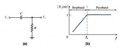
The Bode plot of the voltage gain magnitude is shown in [link]a. The circuit is called a high-pass filter.
[link](a) is another example of a simple RC network. Here, the voltage transfer function is
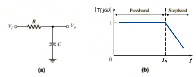
The Bode plot of the voltage gain magnitude for this circuit is shown in [link](b). This circuit is called a low-pass filter.
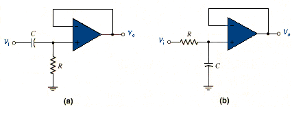
Although these circuits both perform a basic filtering function, they may suffer from loading effects, substantially reducing the magnitude gain from the unity value shown in [link](b) and [link](b). Also, the cutoff frequency and may change when a load is connected to the output. The loading effect can essentially be eliminated by using a voltage follower as shown in [link]. In addition, a non-inverting amplifier configuration can be incorporated to increase the gain, as well as eliminate the loading effects.
These two filter circuits are called one-pole filters; the slope of the voltage gain magnitude curve outside the passband is 6 dB/octave or 20 dB/decade. This characteristic is called the rolloff. The rolloff becomes sharper or steeper with higher-order filters and is usually one of the specifications given for active filters.
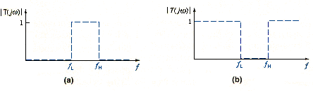
Two other categories of filters are bandpass and band-reject. The desired ideal frequency characteristics are shown in [link]
General Two-Pole Active Filter
Consider [link] with admittances through and an ideal voltage follower. We will derive the transfer function for the general network and will then apply specific admittances to obtain particular filter characteristics.
A KCL equation at node yields
A KCL equation at node produces
From the voltage follower characteristics, we have . Therefore, [link] becomes
Substituting [link] into [link] and again noting that , we have
Multiplying [link] and rearranging terms, we get the following expression for the transfer function:
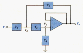
To obtain a low-pass filter, both and must be conductances, allowing the signal to pass into the voltage follower at low frequencies. If element is a capacitor, then the output rolloff at high frequencies.
To produce a two-pole function, element must also be a capacitor. On the other hand, if elements and are capacitors, then the signal will be blocked at low frequencies but will be passed into the voltage follower at high frequencies resulting in a high-pass filter. Therefore, admittances and must both be conductances to produce a two-pole high-pass transfer function.
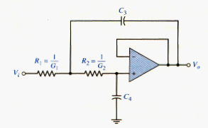
Two-Pole Low-Pass Butterworth Filter
To form a low-pass filter, we set , , and , as shown in [link]. The transfer function, from [link], becomes
At zero frequency, s = j = 0 and the transfer function is
In the high frequency limit, and the transfer function approaches zero. This circuit therefore acts as a low-pass filter.
A butterworth filter is a maximally flat magnitude filter. The transfer function is designed such that the magnitude of the transfer function is as flat as possible within the passband of the filter. This objective is achieved by taking the derivatives of the transfer function with respect to frequency and setting as many as possible equal to zero at the center of the passband, which is at zero frequency for the low-pass filter.
Let . the transfer function is then
We define time constant as and . If we then set s = j , we obtain
The magnitude of the transfer function is therefore
For the maximally flat filter (that is, a filter with a minimum rate of change), which defines a Butterworth filter, we set
Taking the derivative, we find
Setting the derivative equal to zero at yields
[link] is satisfied when , or
Based on this condition, the transfer function magnitude is, from [link],
The 3 dB, or cutoff, frequency occurs when , or when . We then find that
In general, we can write the cutoff frequency in the form
Finally, comparing [link], [link] and [link] yields
and
The two-pole low-pass Butterworth filter is shown in [link](a). The Bode plot of the transfer function magnitude is shown in [link](b). From [link], the magnitude of the voltage transfer function for the two pole low-pass Butterworth filter, can be written as
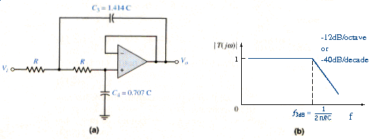
[link] shows that the derivative of the voltage transfer function magnitude at is zero even without setting . However, the added condition of produces the maximally flat transfer characteristics of the Butterworth filter.
Two-Pole High-Pass Butterworth Filter
To perform a high-pass filter, the resistors and capacitors are interchanging from those in the low-pass filter. A two-pole high-pass Butterworth filter is shown in [link](a). The analysis proceeds exactly the same as in the last section, except that the derivative is set equal to zero at . Also, the capacitors are set equal to each other. The 3dB or cutoff frequency can be written in the general form
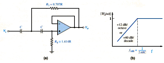
We find that and . The magnitude of the voltage transfer function for the two-pole high-pass Butterworth is
The Bode plot of the transfer function magnitude for the two-pole high-pass Butterworth filter is shown in [link](b).
High-Order Butterworth Filters
The filter order is the number of poles and is usually dictated by the application requirements. An N-pole active low-pass filter has a high-frequency rolloff rate of Nx6 dB/octave. Similarly, the response of an N-pole high-pass filter increases at a rate of Nx6 dB/octave, up to the cutoff frequency. In each case, the 3 dB frequency is defined as
The magnitude of the voltage transfer function for a Butterworth Nth-order low-pass filter is
For a Butterworth Nth-order high-pass filter, the voltage transfer function magnitude is
[link](a) shows a three-pole low-pass Butterworth filter. The three resistors are equal, and the relationship between the capacitors is found by taking the first and second derivatives of the voltage gain magnitude with respect to frequency and setting those derivatives equal to zero at . [link](b) shows a three-pole high-pass Butterworth filter. In this case, the three capacitors are equal and the relationship between the resistors is also found through the derivatives.
Higher-order filters can be created by adding additional RC networks. However, the loading effect on each additional RC circuit becomes more severe. The usefulness of active filters is realized when two or more op-amp filter circuits are cascaded to produce one large higher-order active filter. Because of the low output impedance of the op-amp, there is virtually no loading effect between cascaded stages.
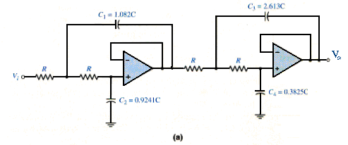
[link](a) shows a four-pole low-pass Butterworth filter. The maximally flat response of this filter is not obtained by simply cascading two two-pole filters. The relationship between the capacitors is found through the first three derivatives of the transfer function. The four-pole high-pass Butterworth filter is shown in [link](b).
Higher-order filters can be designed but are not considered here. Bandpass and band-reject filters use similar circuit configurations.
OSCILLATORS
In this section, we will look at the basic principles of sine-wave oscillators. In our study of feedback, we emphasized the need for negative feedback to provide a stable circuit. Oscillators, however, use positive feedback and, as such, are actually nonlinear circuits in some cases. The analysis and design of oscillator circuits are divided into two parts. In this first part, the condition and frequency for oscillation are determined; in the second part, means for amplitude control is addressed. We consider only the first step in this section to gain insight into the basic operation of oscillators.
Basic Principle of Oscillation
The basic oscillator consists of an amplifier and a frequency-selective network connected in a feedback loop. [link] shows a block diagram the fundamental feedback circuit, in which we are implicitly assuming that negative feedback is employed. Although actual oscillator circuits do not have an input signal, we initially include one here to help in the analysis. In previous feedback circuits, we assumed the feedback transfer function was independent of frequency. In oscillator circuits, however, is the principal portion of the loop gain that is dependent on frequency.
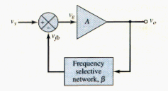
For the circuit shown, the ideal closed-loop transfer function is given by
And the loop gain of the feedback circuit is
We know that the loop gain T(s) is positive for negative feedback, which means that the feedback signal subtracts from the input signal . If T(s) = - 1, the closed-loop transfer function goes to infinity, which means that the circuit can have a finite output for a zero input signal.
As T(s) approaches -1, an actual circuit becomes nonlinear, which means that the gain does not go to infinity. Assume that T(s) = -1 so that positive feedback exists over a particular frequency range. If a spontaneous signal (due to noise) is created at , and the error signal is reinforced and increased. This reinforcement process continues at only those frequencies for which the total phase shift around the feedback loop is zero. Therefore, the condition for oscillation is that, at a specific frequency, we have
The condition that is called the Barkhausen criterion.
[link] shows that two conditions must be satisfied to sustain oscillation:
- The total phase shift through the amplifier and feedback network must be Nx , where N = 0, 1, 2, …,
- The magnitude of the loop gain must be unity.
In the feedback circuit block diagram shown in [link], we implicitly assume negative feedback. For an oscillator, the feedback transfer function, or the frequency-selective network, must introduce an additional 180 degree phase shift such that the net phase around the entire loop is zero. For the circuit to oscillate at a single frequency , the condition for oscillation, from [link], should be satisfied at only that one frequency.
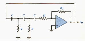
Phase-Shift Oscillator
An example of an op-amp oscillator is the phase-shift oscillator. One configuration of this oscillator circuit is shown in [link]. The basic amplifier of the circuit is the op-amp , which is connected as an inverting amplifier with its output connected to a three-stage RC filter. The voltage followers in the circuit eliminate loading effects between each RC filter stage.
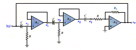
The inverting amplifier introduces a – 180 degree phase shift, which means that each RC network must provide 60 degrees of phase shift to produce 180 degrees required of the frequency-sensitive feedback network in order to produce positive feedback. Note that the inverting terminal of op-amp A3 is at virtual ground; therefore, the RC network between op-amps and functions exactly as the other two RC networks. We assume that the frequency effects of the op-amps themselves occur at much higher frequencies than the response due to the RC networks. Also, to aid in the analysis, we assume an input signal ( ) exists at one node as shown in the figure.
The transfer function of the first RC network is
Since the RC networks are assumed to be identical, and since there is no loading effect of one RC stage on another, we have
where is the feedback transfer function. The amplifier gain A(s) in [link] and [link] is actually the magnitude of the gain, or
The loop gain is then
From [link], the condition for oscillation is that and the phase of must be 180 degrees. When these requirements are satisfied, then v0 will equal ( ) and a separate input signal will not be required.
If we set s = j, [link] becomes
To satisfy the condition , the imaginary component of [link] must equal zero. Since the numerator is purely imaginary, the denominator must become purely imaginary, or which yields
where is the oscillation frequency. At this frequency, [link] becomes
Consequently, the condition is satisfied when
[link] implies that if the magnitude of the inverting amplifier gain is greater than 8, the circuit will spontaneous begin oscillating and will sustain oscillation.
Using [link], we can determine the effect of each RC network in the phase-shift oscillator. At the oscillation frequency , the transfer function of each RC network stage is
which can be written in terms of the magnitude and phase, as follows:
or
as required each RC network introduces a 60 degree phase shift, but they each also introduce an attenuation factor of (1/2) for which the amplifier must compensate.
The two voltage followers shown in the circuit in [link] need not be included in a practical phase shift oscillator. [link] shows a phase shift oscillator without the voltage-follower buffer stages. The three RC network stages and the inverting amplifier are still included. The loading effect of each successive RC network complicates the analysis, but the same principle of operation applies. The analysis shows that the oscillation frequency is
and the amplifier resistor ratio must be
in order to sustain oscillation.
Wien-Bridge Oscillator
Another basic oscillator is the Wien-bridge circuit, shown in [link]. The circuit consists of an op-amp connected in a non-inverting configuration and two RC networks connected as the frequency-selecting feedback circuit.
Again, we initially assume that an input signal exists at the non-inverting terminal of the op-amp. Since the non-inverting amplifier introduces zero phase shift, the frequency-selective feedback circuit must also introduce zero phase shift to create the positive feedback condition.
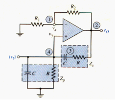
The loop gain is the product of the amplifier gain and the feedback transfer function, or
where and are the parallel and series RC network impedances, respectively. These impedances are
and
Combining [link](a), [link](b) and [link], we get expression for the loop gain function,
Since this circuit has no explicit negative feedback, as was assumed in the general network shown in [link], the condition for oscillation is given by
Since must be real, the imaginary component of [link] must be zero; therefore,
which gives the frequency of oscillation as
The magnitude condition is then
or
[link] (b) states that to ensure the startup of oscillation, we must have (R2/R1) > 2.
Additional Oscillator Configurations
Oscillators that use transistors and LC tuned circuits or crystals in their feedback networks can be used in the hundreds of kHz to hundreds of MHz frequency range. Although these oscillators do not typically contain an op-amp, we include a brief discussion of such circuits for completeness. We will examine the Colpitts, Harley, and crystal oscillators.
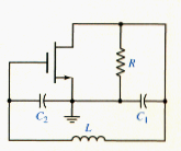
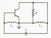
Colpitts Oscillators
The ac equivalent circuit of the Colpitts oscillator with an FET is shown in [link]. A circuit with BJT can be designed. A parallel LC resonant circuit is used to establish the oscillator frequency, and feedback is provided by a voltage divider between capacitors and . Resistor R in conjunction with the transistor provides the necessary gain at resonance. We assume that the transistor frequency response occurs at a high enough frequency that the oscillation frequency is determined by the external elements only.
[link] shows the small-signal equivalent circuit of the Colpitts oscillator. The transistor output resistance r0 can be included in R. A KCL equation at the output node yields
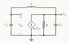
And a voltage divider produces
Substituting [link] into [link], we find that
If we assume that oscillation has started, then and can be eliminated from [link]. We then have
Letting s = j , we obtain
The condition for oscillation implies that both the real and imaginary components of [link] must be zero. From the imaginary component, the oscillation frequency is
which is the resonant frequency of the LC circuit. From the real part of [link], the condition for oscillation is
Combining [link] and [link] yields
where is the magnitude of the gain. [link] states that to initiate oscillations spontaneously, we must have > (C2/C1).
Harley Oscillator
[link] shows the ac equivalent circuit of the Harley oscillator with a BJT. An FET can also be used. Again, a parallel LC resonant circuit establishes the oscillation frequency, and feedback is provided by a voltage divider between inductors and .
The analysis of the Harley oscillator is essentially identical to that of the Colpitts oscillator. The frequency of oscillation, neglecting transistor frequency effects, is
Crystal Oscillator
A piezoelectric crystal, such as quartz, exhibits electromechanical resonance characteristics in response to a voltage applied across the crystal. The oscillations are very stable over time and temperature coefficients on the order of 1 ppm per . The oscillation frequency is determined by the crystal dimensions. This means that crystal oscillators are fixed-frequency devices.
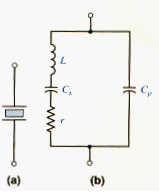
The circuit symbol for the piezoelectric crystal is shown in [link](a), and the equivalent circuit is shown in [link](b). The inductance L can be as high as a few hundred Henrys, the capacitance C, can be on the order of 0.001 pF, and the capacitance can be on the order of a few pF. Also, the Q-factor can be on the order of , which means that the series resistance r can be neglected.
The impedance of the equivalent circuit in [link](b) is
[link] indicates that the crystal has two resonant frequencies, which are very close together. At the series-resonant frequency , the reactance of the series branch is zero; at the parallel-resonant frequency , the reactance of the crystal approaches infinity.
Between the resonant frequencies and , the crystal reactance is inductive, so the crystal can be substituted for an inductance, such as that in a Colpitts oscillator. [link] shows the ac equivalent circuit of a Pierce oscillator, which is similar to the Colpitts oscillator shown in [link] but with the inductor replaced by the crystal. Since the crystal reactance is inductive over a very narrow frequency range, the frequency of oscillation is also confined to this narrow range and is quite constant relative to changes in bias current of temperature. Crystal oscillator frequencies are usually in the range of tens of kHz to tens of MHz.
SCHMITT TRIGGER CIRCUITS
In this section, we will analyze another class of circuits that utilize positive feedback. The basic circuit is commonly called a Schmitt trigger, which can be used in the class of waveform generators called multivibrators. The three general types of multivibrators are: bistable, monostable, and astable. In this section, we will examine the bistable multivibrator, which has a comparator with positive feedback and has two stable states. We will discuss the comparator first, and will then describe various applications of the Schmitt trigger.
Comparator
The comparator is essentially an op-amp operated in an open-loop configuration, as shown in [link](a). As the name implies, a comparator compares two voltages to determine which is larger. The comparator is usually biased at voltages and , although other biases are possible.
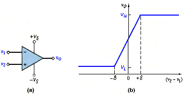
The voltage transfer characteristics, neglecting any offset voltage effects, are shown in [link](b). When is slightly greater than , the output is driven to a high saturated state ; when is slightly less than , the output is driven to a low saturated state . The saturated output voltages and may be close to the supply voltages and , respectively, which means that may be negative. The transition region is the region in which the output voltage is in neither of its saturation states. This region occurs when the input differential voltage is in the range . If, for example, the open-loop gain is 105 and the difference between the two output states is , then
2 = 10/ = V = 0.1 mV
The range of input differential voltage in the transition region is normally very small.
One major difference between a comparator and op-amp is that a comparator need not to be frequency compensated. Frequency stability is not a consideration since the comparator is being driven into one of two states. Since a comparator does not contain a frequency compensation capacitor, it is not slew-rate-limited by the compensation capacitor as is the op-amp. Typical response times for the comparator output to change states are in the range of 30 to 200 ns. An expected response time for a 741 op-amp with a slew rate of 0.7 V/ s would be on the order of 30 s, which is factor of 1000 times greater.
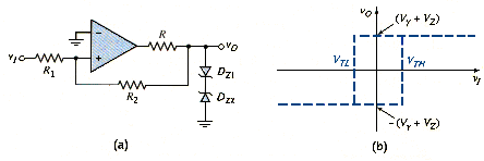
[link] shows two comparator configurations along with their voltage transfer characteristics. In both, the input transition region width is assumed to be negligibly small. The reference voltage may be either positive or negative, and the output saturation voltages are assumed to be symmetrical about zero. The crossover voltage is defined as the input voltage at which the output changes states.
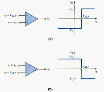
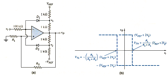
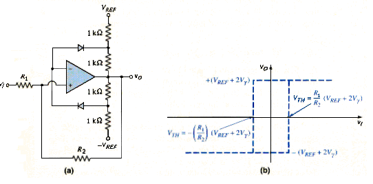
Two other comparator configurations, in which the crossover voltage is a function of resistor ratios, are shown in [link]. Input bias current compensation is also included in this figure. From [link](a), we use superposition to obtain
The ideal crossover voltage occurs when , or
Which can be written as
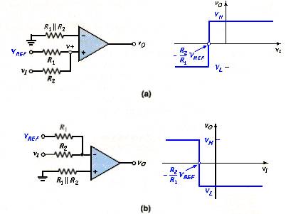
The output goes high when . From [link], we see that v0 = high when is greater than the crossover voltage. A similar analysis produces the characteristics shown in [link](b).
[link] shows one application of a comparator, to control street lights. The input signal is the output of a photodetector circuit. Voltage is directly proportional to the amount of light incident on the photodetector. During the night, , and is on the order of ; the transistor turns on. The current in the relay switch then turns the street lights on. During the day, the light incident on the photodetector produces an output signal such that . In this case, v0 is on the order of , and the transistor turns off.
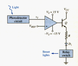
Diode is used as a protection device, preventing reverse bias breakdown in the B-E junction. With zero output current, the relay switch is open and the street lights are off. At dusk and dawn, .
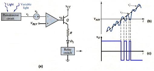
The open-loop comparator circuit shown in [link] may exhibit unacceptable behavior in response to noise in the system. [link](a) shows the same comparator circuit, but with a variable light source, such as clouds causing the light intensity to fluctuate over a short period of time. A variable light intensity would be equivalent to a noise source in series with the signal source . If we assume that is increasing linearly with time (corresponding to dawn), then the total input signal versus time is shown in [link](b). When , the output switches low; when , the output switches high, producing a chatter effect in the output signal as shown in [link](c). This effect would turn the street lights off and on over a relatively short time period. If the amplitude of the noise signal increases, the chatter becomes more severe. This chatter can be eliminated by using a Schmitt trigger.
Basic Inverting Schmitt Trigger
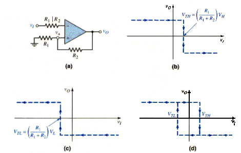
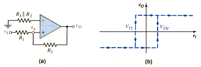
The Schmitt trigger or bistable multivibrator uses positive feedback with a loop-gain greater than unity to produce a bistable characteristic. [link](a) shows one configuration of a Schmitt trigger. Positive feedback occurs because the feedback resistor is connected between the output and noninverting input terminals. Voltage , in terms of the output voltage, can be found by using a voltage divider equation, to yield
Voltage does not remain constant, it is a function of the output voltage. Input signal is applied to the inverting terminal.
Additional Schmitt Trigger Configurations
Voltage transfer characteristics
To determine the voltage transfer characteristics, we assume that the output of the comparator is in one state, namely , which is the high state. Then
As long as the input signal is less than , the output remains in its high state. The crossover voltage occurs when , and is defined as . We have
When is greater than , the voltage at the inverting terminal is greater than that at the noninverting terminal. The differential input voltage ( = ) is amplified by the open-loop gain of the comparator, and the output switches to its low state, or . Voltage then becomes
Since , the input voltage is still greater than , and the output remains in its low state as continues to increase. This voltage transfer characteristic is shown in [link](b). Implicit in these transfer characteristics is the assumption that is positive and is negative.
Now consider the transfer characteristic as decreases. As long as vi is larger than , the output remains in its low saturation state. The crossover voltage now occurs when , and is defined as . We have
As drops below this value, the voltage at the noninverting terminal is greater than that at the inverting terminal. The differential voltage at the comparator terminals is amplified by the open-loop gain, and the output switches to its high state, or . As continues to decrease, it remains less than , therefore, remains in its high state. This voltage transfer characteristic is shown in [link](c).
Complete voltage transfer and bistable characteristics
The complete voltage transfer characteristics of the Schmitt trigger shown in [link](a) combine the characteristics shown in [link](b) and [link](c). These complete characteristics are shown in [link](d). As shown, the crossover voltages depend on whether the input voltage is increasing or decreasing. The complete transfer characteristics therefore show a hysteresis effect. The width of the hysteresis is the difference between the two crossover voltages and .
The bistable characteristic of the circuit occurs around the point , at which the output may be in either its high or low state. The output remains in either state as long as remains in the range . The output switches states only if the input increases above or decreases below .
The complete voltage transfer characteristics given in [link](d) show the inverting characteristics of this particular Schmitt trigger. When the input signal becomes sufficiently positive, the output is in its low state; when the input signal is sufficiently negative, the output is its high state. Since the input signal is applied to the inverting terminal of comparator, this characteristic is as expected.
Additional Schmitt Trigger Configurations
A noninverting Schmitt trigger can be designed by applying the input signal to the network connected to the comparator noninverting terminal. Also, both crossover voltages of a Schmitt trigger circuit can be shifted in either a positive or negative direction by applying a reference voltage. We will study these general circuit configurations, the resulting voltage transfer characteristics, and an application of a Schmitt trigger circuit in this section.
Noninverting Schmitt trigger circuit
Consider the circuit shown in [link](a). The inverting terminal is held essentially at ground potential, and the input signal is applied to resistor , which is connected to the comparator noninverting terminal. Voltage at the noninverting terminal then becomes a function of both the input signal and the output voltage . using superposition, we find that
If is negative and the output is in its low state, then (assumed to be negative), is negative, and the output remains in its low saturation state. Crossover voltage occurs when = 0 and , or, from [link],
Which can be written
Since is negative, is positive.
If we let , where is a small positive voltage; the input voltage is just greater than the crossover voltage and [link] becomes
[link] then becomes
Or
When > 0, the output switches to its high saturation state.
The lower crossover voltage occurs when = 0 and . From [link], we have
Which can be written
Since > 0, then < 0.
The complete voltage transfer characteristics are shown in [link]b. We again note the hysteresis effect and the bistable characteristic around . With sufficiently positive, the output is in its high state; with sufficiently negative, the output is in its low state. The circuit thus exhibits the noninverting transfer characteristic.
Schmitt trigger circuits with applied reference voltage
The switching voltage of a Schmitt trigger is defined as the average value of and . For the two circuits considered in [link](a) and [link](a), the switching voltages are zero, assuming . In some applications, the switching voltage must be either positive or negative direction by applying a reference voltage.
[link](a) shows an inverting Schmitt trigger with a reference voltage . The complete voltage transfer characteristics are shown in [link](b). The switching voltage , assuming and are symmetrical about zero, is given by
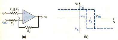
Note that the switching voltage is not the same as the reference voltage. The upper and lower crossover voltages are
And
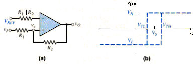
A noninverting Schmitt trigger with a reference voltage is shown in [link](a), and the complete voltage transfer characteristics are shown in [link](b). The switching voltage , again assuming and are symmetrical about zero is given by
and the upper and lower crossover voltages are
And
If the output saturation voltages are symmetrical such that , then crossover voltages are symmetrical about the switching voltage .
Schmitt Trigger Application
Let us reconsider the street light control circuit shown in [link](a) which included a noise source. [link](a) shows the same basic circuit, except that a Schmitt trigger is used instead of a simple comparator.
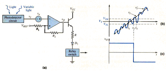
The input signal is again assumed to increase linearly with time. The total input signal is with the noise signal superimposed, as shown in [link](b). At time , the input signal becomes greater than the switching voltage . The output, however, does not switch, since . This means that the input signal is less than the upper crossover voltage. At time , the input signal becomes larger than crossover voltage, or , and the output signal switches from its high to its low state. At time , the input signal drops below , but the output does not switch states since . This means that the input signal remains greater than the lower crossover voltage. The Schmitt trigger circuit thus eliminates the chatter effect which occurs in the output voltage response results directly from the hysteresis effect in the Schmitt trigger characteristics.
Schmitt Trigger with Limiters
In the Schmitt trigger circuits, we have thus far considered, the open-loop saturation voltages of the comparator may not be very precise and may also vary from one comparator to another. The output saturation voltages can be controlled and made more precise by adding limiter networks.
A direct approach at limiting the output is shown in [link]. Two back-to-back Zener diodes are connected between the output and ground. Assuming the two diodes are matched, the output is limited to either the positive or negative value of ( ), where is forward diode voltage and is the reverse Zener voltage. Resistor R is chosen to produce a specified current in the diodes.
Another Schmitt trigger with a limiter is shown in [link](a). If we assume that and is its high state, then is on and is off. Neglecting currents in 100 k resistor, we have , where is the forward diode voltage. We can write
Solving for yields
which means that the output voltage can be controlled and can be designed more accurately. The ideal hysteresis characteristics for this Schmitt trigger are shown in [link](b). As increases or decreases, a small current flows in the 100 k resistor, producing a nonzero slope in the voltage transfer characteristics. The slope is on the order of 1/100, which is quite small.
A noninverting Schmitt trigger with a limiting network is shown in [link](a), and the resulting voltage transfer characteristics are given in [link](b).
NONSINUSOIDAL OSCILLATORS AND TIMING CIRCUITS
Many applications, especially digital electronic systems, use a nonsinusoidal square wave oscillator to provide a clock signal for the system. This type of oscillator is called an astable multivibrator. In other applications, a simple pulse of known height and width is used to initiate a particular set of functions. This type of oscillator is called a monostable multivibrator. First, we will examine the Schmitt trigger connected as an oscillator. Although used extensively in digital electronic systems, these circuits are included here as comparator circuit applications.
Schmitt Trigger Oscillator
The Schmitt trigger can be used in an oscillator circuit to generate a squarewave output signal. This is accomplished by adding an RC network to the negative feedback loop of the Schmitt trigger as shown in [link]. As we will see, this circuit has no stable states. It is therefore called an astable multivibrator.
Initially, we set and equal to the same value, or = = R. we assume that the output switches symmetrically about zero volts, with the high saturated output denoted by and the low saturated output denoted by . If v0 is low, , the . When v drops just slightly below , the output switches high so that and . The network sees a positive step-increase in voltage so capacitor begins to charge and voltage starts to increase toward a final value of .
The general equation for the voltage across a capacitor in an RC network is
Where is the initial capacitor voltage at t = 0, is the final capacitor voltage at t = , and is the time constant. We can now write
Or
where . voltage increase exponentially with time toward a final voltage . However, when becomes just slightly greater than , the output switches to its low state of and . The network sees a negative step-change in voltage, so capacitor now begins to discharge and voltage starts to decrease toward a final value of . We can now write
or
where is the time at which the output switches to its low state. The capacitor voltage then decreases exponentially with time. When decreases to , the output again switches to its high state. The progress continues to repeat itself, which means that this positive-feedback circuit oscillates producing a square wave output signal. [link] shows the output voltage and the capacitor voltage versus time.
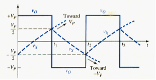
Time can be found from [link] by setting t = when , or
Solving for , we find that
From a similar analysis using [link], we find that the difference between and is also ; therefore, the period of oscillation T is
And the frequency of oscillation is
As an example of an application of this circuit, a variable frequency oscillator is created by letting be a variable resistor.
The duty cycle of the oscillator is defined as the percentage of time that the output voltage is in its high state. For the circuit just considered, the duty cycle is 50 percent, as seen in [link]. This is a result of the symmetrical output voltages and . If asymmetrical output voltages are used, then the duty cycle changes from the 50 percent value.
Monostable Multivibrator
A monostable multivibrator has one stable state, in which it can remain indefinitely if not disturbed. However, a trigger pulse can force the circuit into a quasi-stable state for a definite time, producing an output pulse with a particular height and with. The circuit then returns to its stable state until another trigger pulse is applied. The monostable multivibrator is also called a one shot.
A monostable multivibrator is created by modifying the Schmitt trigger oscillator as shown in [link]. A clamping diode connected in parallel with . In the stable state, the output is high and voltage is held low by the conducting diode .
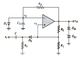
The trigger circuit is composed of the capacitor , resistor , and diode , and is connected to the non-inverting terminal of the comparator. The value of is chosen to be much larger , so that voltage is determined primarily by a voltage divider of and . We then have
Where is the sum of the forward and breakdown voltage of and or . This voltage is positive saturated output voltage.
The circuit is triggered by a negative going step voltage applied to capacitor . This action forward biases diode , and pulls the voltage below . Since the comparator the sees a larger voltage at the inverting terminal, the output switches to its low state of
Voltage then becomes
Causing to become reverse biased, thus isolating the oscillator circuit from the input triggering network. The negative step change in causes voltage to decrease exponentially with a time constant of toward a final value of . Diode is reverse biased during this time. When drops just below the saturated value of given by [link], the output switches back to its positive saturated value of . When reaches , diode again becomes forward biased, is clamped at , and the output remains in its high state.
The waveform of and versus time are shown in [link]. After the output has switched back to the high state, the capacitor voltage must return to its quiescent value of . This implies that there is a recovery time of (T’-T) during which the circuit should not be retriggered.
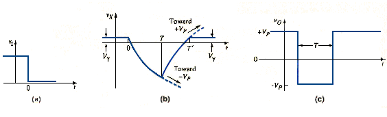
For t > 0, voltage can be written in the same general form as [link], as follows:
where . At t = T, and the output switches high. The pulse width is then
If we assume and if we let , such that , then the pulse width is T = 0.69 . we can show that for and , the recovery time is (T’ – T) = 0.4 . There are alternative circuits with shorter recovery times, but we will not consider them here.
SUMMARY
This chapter presents several applications of op-amps and comparators that may be fabricated as integrated circuits. The circuits considered were: active filters, oscillators, Schmitt triggers, multibrators.
The discussion of active filters was limited to two classes: Butterworth filters and switched-capacitor filters. Butterworth filters have a maximally flat response pass-band. A detailed analysis of the two-pole low-pass Butterworth filter demonstrated that the maximally flat response is obtained by setting the derivatives or the transfer function with respect to frequency equal to zero in center of the pass-band. We determined the relationship between the various resistances and capacitances that produce the required cutoff frequency. High-pass and higher-order Butterworth filters were discussed, and the voltage transfer functions as a function of frequency were given.
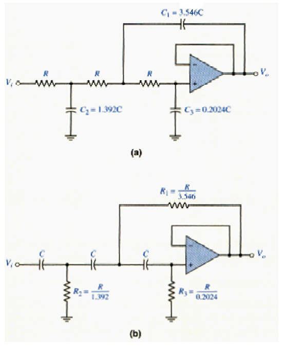
A switched-capacitor filter offers the advantage of an all-IC, since this configuration uses small capacitance value in conjunction with MOS switching transistors that simulate large resistance values. We investigated the basic principle of the switched capacitor technique and applied it to a one-pole low-pass filter, showing that the filter gain and cutoff frequency are functions of capacitor ratios and a clock frequency.
The basic principles for oscillation are: 1) the net phase through the amplifier and feedback network must be zero, and 2) the magnitude of the loop gain must be unity. In order to design an oscillator, the loop gain of a feedback network must provide sufficient phase shift to produce positive feedback. We analyzed several oscillator circuits, including the phase-shift and Wien-bridge oscillators, which use op-amps. The Colpitts, Hartley, and crystal oscillator circuits, which can provide high-frequency oscillations, were also examined, even though these currents tend to use discrete transistors rather than op-amps.
A comparator is essentially an op-amp operated in an open-loop configuration. Since the output of a comparator is driven into either a low or high state, the comparator need not be frequency compensated, hence, it is not as severely slew-rate limited as an op-amp. Typical response times for the output to change states are in the range of 30 to 200 ns.
The Schmitt trigger uses a comparator with positive feedback, which produces a hysteresis in the voltage transfer characteristics. This circuit, with its hysteresis characteristic, can eliminate the chatter effect in an output signal during switching applications in which noise is superimposed on the input signal.
A square-wave generator or oscillator can be produced by incorporating an RC network in negative feedback loop of a Schmitt trigger. This type of oscillator is called an astable multivibrator.