This module presents the basic concepts of MOSFET digital logic circuits. We will examine NMOS logic circuits, which contain only n-channel transistors, and complementary MOS, or CMOS, logic circuits, which contain both n-channel and p-channel transistors. JFET logic circuits are very specialized and therefore not considered here.
The NMOS inverter is the basic of NMOS digital logic circuits. We will analyze the dc voltage transfer characteristics of several inverter designs. We will also define and develop the noise margin of NMOS digital circuits in terms of the inverter voltage transfer curve. We will then determine the impact of the body effect on the dc voltage transfer curve and the logic levels. A transient analysis of the NMOS inverter will determine the propagation delay time in NMOS logic circuits. We will then develop and analyze basic NMOS NOR and NAND logic gates, as well as circuits that perform more complex logic functions.
The CMOS inverter is the basic of CMOS logic gates. We will analyze the inverter dc voltage transfer characteristics, and will determine the power dissipation in the CMOS inverter, demonstrating the principle advantage of CMOS inverter over NMOS circuits. Next, we will develop the noise margin of the CMOS inverter, and then will develop and analyze basic CMOS NOR and NAND logic gates. Finally, we will look at more advanced clocked CMOS logic circuits which eliminate almost half of transistors in a conventional CMOS logic design while maintaining the low power advantage of the CMOS technology.
In a digital system, a transistor can act as a switch between a driving circuit and a load circuit. An NMOS transistor that performs this function is called an NMOS transmission gate; the corresponding CMOS configuration is a CMOS transmission gate. These transmission gates, or pass transistors, can also be configured to perform logic functions, and the circuits are called NMOS-pass or CMOS-pass networks. We will discuss the basics of these networks.
Finally in this module, we will consider a few examples of sequential logic circuits. Two dynamic shift registers are defined and analyzed, and a static R-S flip-flop are defined and analyzed.
NMOS INVERTERS
The inverter is the basic circuit of most MOS logic circuits. The design techniques used in NMOS logic circuits are developed from the dc analysis results for NMOS inverter. Extending the concepts developed from the inverter to NOR and NAND gates is then direct. Alternative inverter load elements are compared in terms of power consumption, packing density, and transfer characteristics. The transient analysis and switching characteristics of the inverters give an indication of the propagation delay times of NMOS logic circuits.
n-Channel MOSFET
In this section, we will quickly review the n-channel MOSFET characteristics, emphasizing specific properties important in digital circuit design.
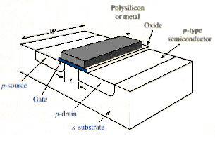
A simplified n-channel MOSFET is shown in [link]. The body or substrate, is a single crystal silicon wafer which is the starting material for circuit fabrication and provides physical support for the integrated circuit. The active transistor region is the surface of the semiconductor and is comprised of the heavy doped source and drain regions and p-type channel region. The channel length is L and the channel width is W. normally, in any given fabrication process, the channel length is the same for all transistors, while the channel width is variable.

[link]b shows a more detailed view of the n-channel MOSFET. This figure demonstrates that the actual device geometry is more complicated than that indicated by the simplified cross section.
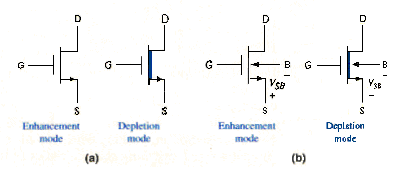
[link]a shows the simplified circuit symbols for the n-channel enhancement and depletion-mode devices. When we explicitly consider the body or substrate connection, we will use the symbols shows in [link]b.
In an integrated circuit, all n-channel transistors are fabricated in the same p-type substrate material. The substrate is connected to the most negative potential in the circuit, which for digital circuits, is normally at ground potential or zero volts. However, the source terminal of many of transistors will not be at zero volts, which means that a reverse-biased pn junction will exist between source and substrate.
When the source and body terminal are connected together, the threshold voltage, to a first approximation, is independent of the applied voltages. However, when the source and body voltages are not equal, as when transistors are used for active loads, for instance, the threshold voltage is a function of difference between these voltages. We can write
where is the source-to-body voltage, and is the threshold voltage for zero source-to-body voltage or . The parameter is the p-type substrate doping concentration, is the semiconductor permittivity, is the oxide capacitance per unit area, is a potential related to the substrate doping concentration, and is the body-effect coefficient.
The current-voltage characteristics of the n-channel MOSFET are functions of both the electrical and geometrical properties of the device. When the transistor is biased in the nonsaturation region, for and , we can write
In the saturation region, for , and , we have
The transition point separates the non-saturation and saturation regions and is the drain-to-source saturation voltage which is given by
The term is sometimes included in [link]b to account for channel length modulation and the finite output resistance. In most cases, it has little effect on the operating characteristics of MOS digital circuits. In our analysis, the term is assumed to be zero unless otherwise stated.
The parameter is the NMOS transistor conduction parameter and is given by
The electron mobility and oxide capacitance are assumed to be constant for all devices in a particular IC.
The current-voltage characteristics are directly related to the channel width-to-length ratio, or the size of the transistor. In general, in a given IC, the length L is fixed, but the designer can control the channel width W.
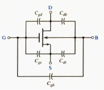
Since the MOS transistor is a majority carrier device, the switching speed of MOS digital circuits is limited by the time required to charge or discharge the capacitances between device electrodes and between interconnect lines and ground. [link] shows the significant capacitances in a MOSFET. The capacitances and are the source-to-body and drain-to-body p junction capacitances. The total input gate capacitance, to a first approximation, is a constant equal to
where is the oxide capacitance per unit area, and is a function of the oxide thickness. The parameter also appears in the expression for the conduction parameter.
NMOS Inverter Transfer Characteristics
Since the inverter is the basic for most logic circuits, we will describe the NMOS inverter and will develop the dc transfer characteristics for three types of inverters with different load devices. This discussion will introduce voltage transfer functions, noise margins, and the transient characteristics of FET digital circuits.
NMOS inverter with resistor load
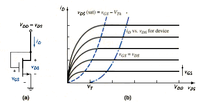
[link]a shows a single NMOS transistor connected to a resistor to form an inverter. The transistor characteristics and load line are shown in [link]b, along with the parametric curve separating the saturation and nonsaturation regions. We determine the voltage transfer characteristics of the inverter by examining the various regions in which the transistor can be biased.
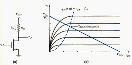
When the input voltage is less than or equal to the threshold, or , the transistor is cut off, , and the output voltage is . The maximum output voltage is defined as the logic 1 level. As the input voltage becomes just greater than , the transistor turns on and is biased in the saturation region. The output voltage is than
Where the drain current is given by
Combining [link] and [link] yields
which relates the output and input voltages as long as the transistor is biased in the saturation region.
As the input voltage increases, the Q-point of the transistor moves up the load line. At the transition point, we have
where and are the drain-to-source and gate-to-source voltage, respectively, at the transition point. Substituting [link] into [link], the input voltage at the transition point is the determined from
As the input voltage becomes greater than , the Q-point continues to move up the load line, and the transistor becomes biased in the nonsaturation region. The drain current is then
Combining [link] and [link] yields
Which relates to the input and output voltage as long as the transistor is biased in the nonsaturation region.
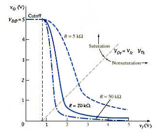
[link] shows the voltage transfer characteristics of this inverter for three resistor values. Also shown is the line, given by [link], which separates the saturation and nonsaturation bias region of the transistor. The figure shows that the minimum output voltage, or the logic 0 level, for a high input decreases with increasing load resistance, and the sharpness of the transition region between a low input and a high input increases with increasing load resistance.
It should be note that a large resistance is difficult to fabricate in an IC. A large resistor value in the inverter will limit current and power consumption as well as provide a small value. But it would also require a large chip area if fabricated in a standard MOS process. To avoid this problem, MOS transistors can be used as load devices, replacing the resistor, as discussed in subsequent paragraphs.
NMOS inverter with enhancement load
An n-channel enhancement-mode MOSFET with the gate connected to the drain can be used as a load device in an NMOS inverter. [link]a shows such a device. For , the drain current is zero. For , a nonzero drain current is induced in the device. We can see that the following condition is satisfied:
A transistor with this connection always operates in the saturation region when not in cutoff.
The drain current is
We continue to neglect the effect of the output resistance and the parameter. The versus characteristic is shown in [link]b which indicates that this device acts as a nonlinear resistor.
[link]a shows an NMOS inverter with the enhancement load device. The driver transistor parameters are denoted by and . The substrate connections are not shown. In the following analysis, we neglect the body effect and we assume all threshold voltages are constant. These assumptions do not seriously affect the basic analysis or the inverter characteristics.
The driver transistor characteristics and the load curve are shown in [link]b. When the inverter input voltage is less than the driver threshold voltage, the driver is cut off and the drain currents are zero. From [link], we have
From [link]a, we see that , which means that
The maximum output voltage is then
For the enhancement load NMOS inverter, the maximum output voltage, which is the logic 1 level, does not reach the full value. This cutoff point is shown on the load curve in [link]b.

As the input voltage becomes just greater than the driver threshold voltage , the driver transistor turns on and is biased in the saturation region. In steady-state, the two drain currents are equal since the output will be connected to the gates of other MOS transistors. We have , which can be written as
[link] is expressed in terms of the individual transistor parameters. In terms of the input and output voltages, the expression becomes
Solving for the output voltage yields
As the input voltage increases, the driver Q-point moves up the load curve and the output voltage deceases linearly with .
At the driver transition point, we have
or
Substituting [link] into [link], we find the input voltage at the transition point, which is
As the input voltage becomes greater than , the driver transistor Q-point continues to move up the load curve and the driver becomes biased in the nonsaturation region. Since the driver and load drain currents are still equal, or , we now have
Writing [link] in terms of the input and output voltages produces
Obviously, the relationship between and in this region is not linear.
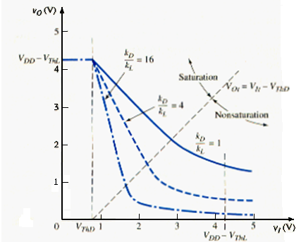
[link] shows the voltage transfer characteristics of this inverter for three -to- ratios. The ratio is the aspect ratio and is related to the width-to-length parameters of the driver and load transistors.
The line, given by [link], separating the driver saturation and nonsaturation regions is also shown in the figure. We see that the minimum output voltage, or the logic 0 level, for a high input decreases with an increasing ratio. As the width-to-length ratio of the load transistor decreases, the effective resistance increases, which means that the general behavior of the transfer characteristics is the same as for the resistor load. However, the high output voltage is
When the driver is biased in the saturation region, we find the slope of the transfer curve, which is the inverter gain, by taking the derivative of [link] with respect to . We see that
When the aspect ratio is greater than unity, the inverter gain magnitude is greater than unity. A logic circuit family with an inverter transfer curve that exhibits a gain greater than unity for some region is called a restoring logic family. Restoring logic is so named because logic signals that are degraded for some reason in one circuit can be restored by gain of subsequent logic circuits.
NMOS inverter with depletion load
Depletion mode MOSFET can also be used as load elements in NMOS inverters. [link]a shows the NMOS inverter with depletion load. The gate and source of the depletion mode transistor are connected together. The driver transistor is still an enhancement-mode device. As before, the driver transistor parameters are ( > 0) and , and the load transistor parameters are ( < 0) and . Again, the substrate connections are not shown. The fabrication process for this inverter is slightly more complicated than for the enhancement-load inverter, since the threshold voltages of the two devices are not equal. However, as we will see, the advantage of the inverter makes the extra processing steps worthwhile. This inverter has been the basic of many microprocessor and static memory designs.
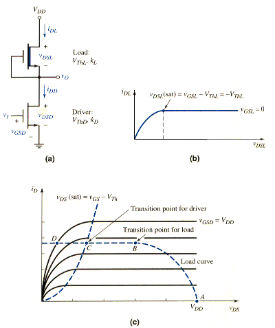
The current-voltage characteristic curve for the depletion load, neglecting the body effect, is shown in [link]b. Since the gate is connected to the source, , and the Q-point of the load is on this particular curve.
The driver transistor characteristics and the ideal load curve are shown in [link]c. When the inverter input is less than the driver threshold voltage, the driver is cut off and the drain currents are zero. From [link]b, we see that for , the drain-to-source voltage of the load transistor must be zero; therefore, for . An advantage of the depletion load inverter over the enhancement-load inverter is that the high output voltage, or the logic 1 level, is at the full value.
As the input voltage becomes just greater than the driver threshold voltage , the driver turns on and is biased in the saturation region; however, the load is biased in the nonsaturation region. The Q-point lies between points A and B on the load curve shown in Figure 9c. We again set the two drain currents equal, or , which means that
Writing [link] in terms of the input and output voltages yields
This equation relates the input and output voltages as long as the driver is biased in saturation region and the load is biased in the nonsaturation region.
There are two transition points for the NMOS inverter with a depletion load: one for the load and one for the driver. These are points B and C, respectively, in [link]c. The transition point for load is given by
or
Since is negative, the output voltage at the transition point is less than . The transition point for the driver is given by
When the Q-point lies between points B and C on the load curve, both devices are biased in the saturation region, and
or
[link] demonstrates that the input voltage is a constant as the Q-point passes through this region. This effect is also shown in [link]c; the load curve between points B and C lies on a constant curve.
For an input voltage greater than the value given by [link], the driver is biased in the nonsaturation region while the load is biased in the saturation region. The Q-point is now between points C and D on the load curve shown in [link]c. Equaing the two drain currents, we obtain
which becomes
This equation implies that the relationship between the input and output voltages is not linear in this region.
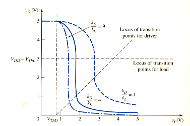
[link] shows the voltage transfer characteristics of this inverter for three values of . Also shown are the loci of transition points for the load and driver transistor as given by [link] and [link], respectively.
CMOS INVERTER
Complementary MOS, or CMOS, circuits contain both n-channel and p-channel MOSFETs. As we will see, the power dissipation in CMOS logic circuits is much smaller than in NMOS circuits, which makes CMOS very attractive. We will briefly review the characteristics of p-channel transistors, and will then analyze the CMOS inverter, which is the basic of most CMOS logic circuits. We will examine the CMOS NOR and NAND gates and other basic CMOS logic circuits, covering power dissipation, noise margin, fanout, and switching characteristics.
p-Channel MOSFET
[link] shows a simplified view of p-channel device. Again, the channel length is L and the channel width is W. Usually in any given fabrication process, the channel length is the same for all devices, so the channel width W is the variable in logic circuit design.
[link]a shows the simplified circuit symbol for the p-channel enhancement-mode device. When the body or substrate connection is needed, we will use the symbol shown in [link]b. Usually, the p-channel depletion-mode device is not used in CMOS digital circuits; therefore, it is not addressed here.

Normally, in an integrated circuit, more than one p-channel device will be fabricated in the same n-substrate so the p-channel transistors will exhibit a body effect. The n-substrate is connected to the most positive potential. The source terminal may be negative with respect to the substrate, therefore, voltage VBS may exist between the body and the source. The threshold voltage is
where is the threshold voltage for zero body-to-source voltage, or . The parameter is the n-substrate doping concentration and is the potential related to the substrate doping. The parameter is the body effect coefficient.
The current-voltage characteristics of the p-channel MOSFET are functions of both the electrical and geometric properties of the device. When the transistor is biased in the nonsaturation region; we have . Therefore,
In the saturation region, we have , which means that
The gate potential is negative with respect to the source. For the p-channel transistor to conduct, we must have , where is negative for an enhancement-mode device. We also see that when the p-channel device is conducting.
In most cases, the channel length modulation factor has very little effect on the operating characteristics of MOS digital circuits. Therefore, the term is assumed to be zero unless otherwise stated.
The transition point, which separates the nonsaturation and saturation bias region, is given by
The parameter is the conduction parameter and given by
As before, the hole mobility and oxide capacitance are assumed to be constant for all devices. The hole mobility in p-channel silicon MOSFETs is approximately one-half the electron mobility in n-channel silicon MOSFETs. This means that a p-channel device must be approximately twice as large as that of an n-channel device in order that the two devices be electrically equivalent (that is, that they have the same conduction parameter values).
DC Analysis of the CMOS Inverter
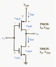
The CMOS inverter, shown in [link], is a series combination of a p-channel and an n-channel MOSFET. The gates of the two MOSFETs are connected together to form the input and the two drains are connected together to form the output. Both transistors are enhancement-mode devices. The parameters of the NMOS are denoted by and , where > 0, and the parameters of the PMOS are denoted by and , where < 0.
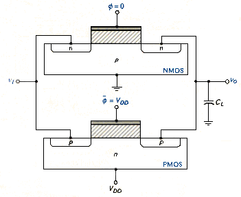
[link] shows a simplified cross section of a CMOS inverter. In this process, a separate p-well region is formed within the starting n-substrate. The n-channel device is fabricated in the p-well region and the p-channel device is fabricated in n-substrate. Although other approaches, such as an n-well in a p-substrate, are also used to fabricate CMOS circuits, the important point is that the processing is more complicated for CMOS circuits than for NMOS circuits. However, the advantages of CMOS digital logic circuits over NMOS circuits justify their use.

Voltage Transfer Curve
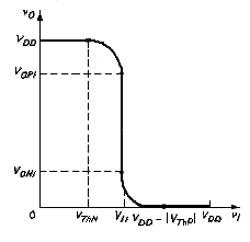
[link] shows the transistor characteristics for both the n- and p-channel devices. We can determine the voltage transfer characteristics of the inverter by evaluating the various transistor bias regions. For , the NMOS device is cut off, , and . The PMOS source-to-gate voltage is which means that the PMOS is biased on the curve marked B in [link]b. Since the only point on the curve corresponding to occurs at , the output voltage is . This condition exists as long as the NMOS transistor is cut off, or .
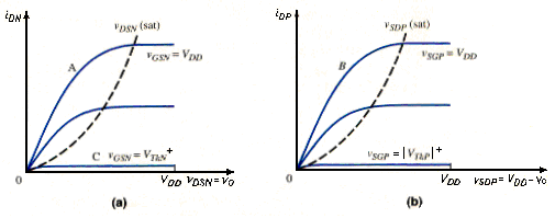
For , the PMOS device is cut off, . The NMOS gate-to-source voltage is and the NMOS is biased on the curve marked A in [link]a. The only point on the curve corresponding to occurs at . The output voltage is zero as long as the PMOS transistor is cut off, or . This means that the input voltage is in the range .
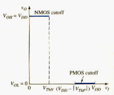
[link] shows the voltage transfer characteristics generated thus far for the CMOS inverter. The more positive output voltage corresponds to a logic 1, or , and the more negative output voltage corresponds to a logic 0, or . When the output is in the logic 1 state, the NMOS transistor is cut off; when the output is in the logic 0 state, the PMOS transistor is cut off.
Ideally, the current in the CMOS inverter in either steady-state condition is zero, which means that, ideally, the quiescent power dissipation is zero. This result is attractive feature of CMOS digital circuits. In actuality, CMOS inverter circuits exhibit a small leakage current in both steady-state conditions due to the reverse-biased pn junctions. However, the power dissipation may be in the nanowatt range rather than in miliwatt range of NMOS inverters. Without this feature, VLSI would not be possible.
When the input voltage is just greater than , or
The NMOS begins to conduct and Q-point falls on the curve marked C in [link]a. The current is small and , which means that the NMOS is biased in the saturation region. The PMOS source-to-drain voltage is small, so the PMOS is biased in the nonsaturation region. Setting , we can write
Relating the gate-to-source and drain-to-source voltages I each transistor to the inverter input and output voltages, respectively, we can rewrite [link] as follows:
[link] relates the input and output voltage as long as the NMOS is biased in the saturation region and the PMOS is biased in the nonsaturation region.
The transition point for the PMOS is defined from
Using [link], [link] can be written
or
Where and are the PMOS output and input voltages, respectively, at the transition point.
The transition point for the NMOS is defined from
or
Where and are the NMOS output and input voltages, respectively, at the transition point.
Keeping in mind that is negative for an enhancement-mode PMOS, [link]b and [link]b are plotted in [link]. We determine the input voltage at the transition points by setting the two drain currents equal to each other when both transistors are biased in the saturation region. The result is
Relating the gate-to-source voltages to the input voltage, [link] becomes
For this ideal case, the output voltage does not appear in [link], and the input voltage is a constant, as long as the two transistors are biased in the saturation region.
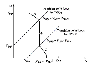
Voltage from [link] is the input voltage at the PMOS and NMOS transition points. Solving for , we find that
For , the NMOS is biased in the nonsaturation region and the PMOS is biased in the saturation region. Again equating the two drain currents, we have
Also, relating the gate-to-source and drain-to-source voltages to the input and output voltages, respectively, modifies [link], as follows:
[link] relates the input and output voltages as long as the NMOS is biased in the nonsaturation region and the PMOS in the saturation region. [link] shows the completed voltage transfer curve.
CMOS Inverter Currents
When the CMOS inverter input voltage is either a logic 0 or a logic 1, the current in the circuit is zero since one of the transistor is off. When the input voltage is in the range , both transistors conducting and a current exists in the inverter.
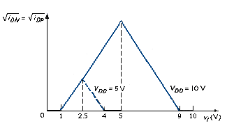
When the NMOS transistor is biased in the saturation region, the current in the inverter is controlled by and the PMOS source-to-drain voltage adjusts such that . This condition is demonstrated in [link]. We can write
Taking the square root yields
As long as the NMOS transistor is biased in the saturation region, the square root of the CMOS inverter is a linear function of the input voltage.
When the PMOS transistor is biased in the saturation region, the current in the inverter is controlled by and the NMOS drain-to-source voltage adjusts such that . This condition is demonstrated in [link]. Using [link], we can write that
Taking the square root yields
As long as the PMOS transistor is biased in the saturation region, the square root of the CMOS inverter current is also a linear function of the input voltage.
[link] shows plots of the square root of the inverter current for two values of bias. These curves are quasi-static characteristics in that no current is diverted into a capacitive load. At the inverter switching point, both transistors are biased in the saturation region and both transistors influence the current. At the switching point, actual current characteristic does not have a sharp discontinuity in the slope. The channel length modulation parameter also influences the current characteristics at the peak values. However, the curves in [link] are excellent approximations.
Power Dissipation
In the quiescent or static state, in which the input is either a logic 0 or logic 1; power dissipation in the CMOS inverter is virtually zero. However, during the switching cycle from one to another, current flows and power is dissipated. The CMOS inverter and logic circuits are used to drive other MOS devices for which the input impedance is a capacitance. During the switching cycle, then, this load capacitance must be charged and discharged.
In [link], the output switches from its low to its high state. The input is switched low, the PMOS gate is at zero volts, and the NMOS is cut off. The load capacitance CL must be charged through the PMOS device. Power dissipation in the PMOS transistor is given by
The current and the output voltage are related
The energy dissipated in the PMOS device as the output switches from low to high is
which yields
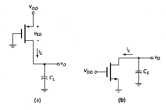
After the output has switched high, the energy stored in the load capacitance is (1/2) . When the inverter input goes high, the output switches low, as shown in [link]b. The PMOS device is cut off, the NMOS transistor conducts and the load capacitance discharges through the NMOS device. All the energy stored in the load capacitance is dissipated in the NMOS. As the output switches from high to low, the energy dissipated in the NMOS transistor is
The total energy dissipated in the inverter during one switching cycle is therefore
If the inverter is switched at frequency, the power dissipated in the inverter is
[link] shows that the power dissipated in a CMOS inverter is directly proportional to the switching frequency and to . The drive in digital IC design is toward lower supply voltages, such as 3 volts or less.
The power dissipation is proportional to . In some digital circuits, such as watches, the CMOS logic circuits are biased at , so the power dissipation is substantially reduced.
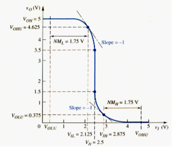
Noise Margin
[link] shows the general voltage transfer function of a CMOS inverter. The parameters and determine the noise margins and are defined as the points at which
which is the same as for the NMOS inverters. For and , the gain is less than unity and the output changes slowly with input voltage. However, when the input voltage is in the range , the inverter gain is greater than unity, and the output signal changes rapidly with a change in the input voltage. This is the undefined range.
The noise margins are defined as
and
Point occurs when the NMOS is biased in saturation region and the PMOS is biased in nonsaturation region. The relationship between the input and output voltages is given by [link]. Taking the derivative with respect to yields
Setting the derivative equal to -1, we have
Solving for v0 produces
Combining [link] and, [link], we see that voltage VIL is
If , [link] becomes indefinite, since a zero would exist in both the numerator and the denominator. However when . [link] becomes
Substituting [link] into [link] yields a voltage VIL of
For .
Point occurs when the NMOS is biased in the nonsaturation region and the PMOS is biased in the saturation region. The relationship between the input and output voltages is given by [link]. Taking the derivative with respect to yields
Setting the derivative equal to -1, we find that
The output v0 is then
Combining [link] and [link], yields VIH as
Again, if , [link] becomes indefinite, since a zero would exist in both the numerator and the denominator. However, when , [link] becomes
Substituting [link] into [link] yields a voltage of
CMOS LOGIC CIRCUITS
Large-scale integrated CMOS circuits are used extensively in digital systems, including watches, calculators, and microprocessors. We will look at the basic CMOS NOR and NAND gates, CMOS transmission gate, and will then analyze more advanced clocked CMOS logic circuits.
Basic CMOS Logic Gates
In the basic or classical CMOS basic circuits, the gates of a PMOS and an NMOS are connected together, and additional PMOS and NMOS transistors are connected in series or parallel to form specific logic circuits. [link]a shows a two-input CMOS NOR gate. The NMOS transistor are in parallel and the PMOS transistors are in series.
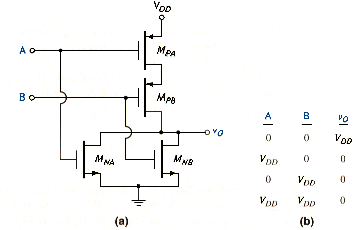
If A = B = 0, then both and are cut off, and the current in the circuit is zero. The source-to-gate voltage of is VDD but the current is zero; therefore, of is zero. This means that the source-to-gate voltage of is also . However, since the current is zero, then of is zero. The output voltage is therefore .
If the input signals are A = logic 1 = and B = logic 0 = 0 V, then the source-to-gate voltage of is zero, and the current in the circuit is again zero. The gate-to-source voltage of is VDD but the current is zero, so of is zero and = 0 = logic 0. This result also holds for the other two possible input conditions, since at least one PMOS is cut off and at least one NMOS is in a conducting state. The NOR logic function is shown in the truth table of [link]b.
A two-input CMOS NAND logic gate is shown in [link]a. In this case, the NMOS transistors are in series and the PMOS transistors are in parallel. If A = B = logic 0, the two NMOS devices are cut off and the current in the circuit is zero. The source-to-gate voltage of each PMOS device is , which means that both PMOS transistors are in a conducting state. However, since the current is zero, vSD for both and is zero and . This result applies if at least one input is a logic 0.
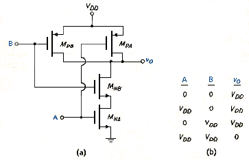
If the input signals A = B = logic 1 = , then both PMOS transistors are cut off, and the current in the circuit is zero. With A = logic 1, is in conducting state; however, since the current is zero, then of is zero. This means that the gate-to-source voltage of is also VDD and is also in a conducting state. However, since the current is zero, then of is zero, and = logic 0 = 0 V. The NAND logic function is shown in the truth table in [link]b.
In both the CMOS NOR and NAND logic gates, the current in the circuit is essentially zero when the inputs are in any quiescent state. Only very small reverse-bias pn junction currents exist. The quiescent power dissipation is therefore essentially zero. Again, this is the primary advantage of CMOS circuits.
To obtain symmetrical switching times or propagation delay times for the high-to-low and low-to-high output transitions, the effective conduction parameters of the complete PMOS and composite NMOS devices must be equal. For the CMOS NOR logic gate shown in [link], we can write
where is the effective conduction parameter of the two parallel NMOS devices and is the effective conduction parameter of the two series PMOS transistors.
The effective channel width of the parallel NMOS devices is twice the individual width; similarly, the effective channel length of the series PMOS devices is twice the individual length. [link] is then
Since , [link] becomes
or
This equation states that in the two-input CMOS NOR gate, the width-to-length ratio of the PMOS transistors must be approximately eight times that the NMOS devices in order to provide the current required for symmetrical switching.
[link] shows the voltage transfer and current characteristics of the two-input CMOS NOR logic gate from a PSpice analysis. [link]a shows the results when the two inputs are tied together; the circuit then behaves as a composite inverter. When the width-to-length ratios of the PMOS devices are eight times those of the NMOS devices, the transfer characteristics are symmetrical as expected.
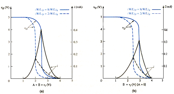
Also shown are the voltage transfer and current characteristics if the p-channel width-to-length ratios are only twice as large as those of the n-channel devices. The resulting switching characteristics are not symmetrical, and the maximum current is significantly reduced, implying that the switching times would be longer for this case.
[link]b shows the transfer characteristics for input A held low and input B varied from zero to . This corresponds to only one input changing states while the other input remains constant. In this case, transistor is on and transistor is cut off. The resulting circuit is essentially equivalent to a simple CMOS inverter. When the width-to-length ratios of the PMOS devices are twice as large as those of the NMOS devices, the transfer characteristics are almost symmetrical, as we would expect for the CMOS inverter. When the PMOS width-to-length ratios are increased, the voltage transfer characteristic is no longer symmetrical. However, the maximum current is larger since the PMOS devices are lager, and this shortens the switching times. These results shown that we obtain good transfer characteristics when for the two-input CMOS NOR circuit.
Clocked CMOS Logic
The CMOS NOR and NAND logic gates presented in the last section are called static circuits because periodic clock signals are not used. In practice, all systems employing sequential logic require clock signal for proper synchronized operation. Static CMOS NOR and NAND gates can be redesigned with an added clocked signal to eliminate many of the PMOS devices, while maintaining the low-power CMOS characteristics. In general, PMOS devices must be larger than NMOS transistors. Eliminating as many PMOS devices as possible reduces the required chip area as well as the input capacitance.
Clocked CMOS circuits are dynamic circuits that generally precharge the output node to a particular level when the clock is at a logic 0. Consider the circuit shown in [link]. When the clock signal is low, or CLK = logic 0, MN1 is cut off and the current in the circuit is zero. Transistor MP1 is in a conducting state, but since the current is zero, then charges to . A high input to the CMOS inverter means that . During this phase of the clock signal, the gate of is precharged.
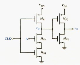
During the next phase, when the clock signal goes high, or CLK = logic 1, transistor cuts off and is biased in a conducting state. If input A = logic 0, then is cut off and there is no discharge path for voltage ; therefore, remains charged at . However, if CLK = logic 1 and A = logic 1, then both and are biased in a conducting state providing a discharge path for voltage . As is pulled out, output signal goes high.
The quiescent power dissipation in this circuit is essentially zero, as it is precharge output , if it has been pulled low during the previous halt clock cycle.
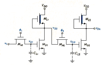
The single NMOS transistor MNA in [link] can be replaced by a more complex NMOS logic circuit. Consider the two circuits shown in [link]. When CLK = logic 0, then MN1 cuts off and MP1 is in its conducting state in both circuits; then and = 0. For the circuit shown in [link]b, when CLK = logic 1, voltage v01 is discharged to ground or pulled low only when A = B = logic 1. In this case, goes high. The circuit in [link]a performs the AND function. Similarly, the circuit in [link]b performs the OR function.
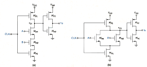
The advantage of the precharge technique is that it avoids the use of extensive pullup networks: only one PMOS and one NMOS transistor are required. This leads to an almost 50-percent saving in silicon area for larger circuits, and a reduction in capacitance resulting in higher speed. In addition, the static or quiescent power dissipation is essentially zero, so the circuit maintains the characteristics of CMOS circuits.
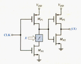
The AND and OR logic transistors and in [link]a and [link]b can be replaced by a generalized logic network as indicated in [link]. The box marked f is an NMOS pull-down network that performs a particular logic function f(X) of n-variables, where X = ( , , .... ). The NMOS circuit is a combination of series-parallel interconnections of n transistors. When the clock signal goes high, the CMOS inverter output is the logic function f(X).
The set of X inputs to the logic circuit f is derived from the outputs of other CMOS inverters and clocked logic circuits. This means that when CLK = logic 0, the outputs of all n-variables X = ( , , .... ) are a logic 0 during the precharge cycle. During this time, all NMOS transistors are cut off, which guarantees that output can be precharged to . There can be only one possible transition at each node during the evaluation phase. The output of the CMOS buffer may change from a 0 to 1.
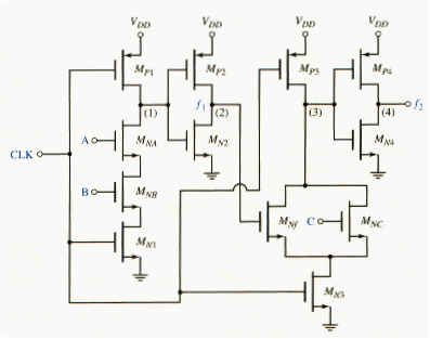
An example of a two-stage domino CMOS circuit is shown in [link]. During the precharge cycle, in which CLK = logic 0, nodes 1 and 3 are charged high and nodes 2 and 4 are low. Also during this time, the inputs A, B, and C are all a logic 0. During the evaluation phase, in which CLK = logic 1, if A = C = logic 1 and B = logic 0, then node 1 remains charged high, = logic 0, and node 3 discharges causing to go high. However, if, during the evaluation phase, A = B = logic 1 and C = logic 0, then node 1 is pulled low causing to go high, which in turn causes node 3 to go low and forces node 4 high. This chain of actions thus leads to the term domino circuit.
Fanout
The term fanout refers to the number of load gates of similar design connected to the output of a driver gate. The maximum fanout is the maximum number of load gates that may be connected to the output. Since the CMOS logic gate will be driving other CMOS logic gates, the quiescent current required to drive the other CMOS gates is essentially zero. In terms of static characteristics, the maximum fanout is virtually limitless.
However, each additional load gate increased the load capacitance that must be charged and discharged as the driver gate changes state, and this places a practical limit on the maximum allowable number of load gates. [link] shows a constant current charging a load capacitance. The voltage across the capacitance is
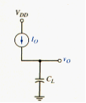
The load capacitance is proportional to the number N of load gates and to the input gate capacitance of each load. The current is proportional to the conduction parameter of the driver transistor. The switching time is therefore
where the gate capacitance is directly proportional to the gate area of the load , and the conduction parameter of the driver transistor is proportional to the width-to-length ratio. [link] can be rewritten as
The propagation delay time, which is proportional to the switching time, increases as the fanout increases. The propagation delay time could be reduced by increasing the size of the driver transistor. However, in any given driver logic circuit and load logic circuit, the sizes of the devices are generally fixed. Consequently, the maximum fanout is limited by the maximum acceptable propagation delay time.
Propagation delay times are typically, measured with a specified load capacitance. The average propagation delay time of a two-input CMOS NOR gate (such as an SN74HC36) is 25 ns, measured with a load capacitance of = 50 pF. Since the input capacitance is CI = 10 pF, a fanout of five would produce a 50 pF load capacitance. A fanout larger than five would increase the load capacitance, and would also increase the propagation delay time above the specified value.
TRANSMISSION GATES
Transistors can act as switches between driving circuits and load circuits. Transistors used to perform this function are called transmission gates. We will examine NMOS and CMOS transmission gates, which can also be configured to perform logic functions.
NMOS Transmission Gate
The NMOS enhancement-mode transistor shown in [link]a is a transmission gate connected to a load capacitance , which could be the input gate capacitance of a MOS logic circuit. In this circuit, the transistor must be bilateral, which means it must be able to conduct current in either direction. This is a natural feature of MOSFETs. Terminals a and b are assumed to be equivalent, and the bias applied to the transistor determines which terminal acts as the drain and which terminal acts as the source. The substrate must be connected to the most negative potential in the circuit, which is usually ground. [link]b shows a simplified circuit symbol for the NMOS transmission gate that is used extensively.
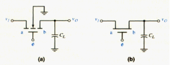
We assume that the NMOS transmission gate is to operate over a voltage range of zero-to- . If the gate voltage is zero, then the n-channel transistor is cut off and the output is isolated from the input. The transistor is essentially an open switch.
If = , , and is initially zero, then terminal a acts as the drain since its bias is , and terminal b acts as the source since its bias is zero. Current enters the drain from the input, changing up the capacitor. The gate-to-source voltage is
As the capacitor charges and v0 increase, the gate-to-source voltage decreases. The capacitor stops charging when the current goes to zero. This occurs when the gate-to-source voltage VGS becomes equal to the threshold voltage . The maximum output voltage occurs when , therefore, from [link], we have
or
where is the threshold voltage taking into account the body effect.
[link]b demonstrates one disadvantage of an NMOS transmission gate. A logic 1 level degrades, or attenuates, as it passes through the transmission gate. However, this may not be a serious problem for many applications.
Now consider the situation in which , , and initially. Terminal b then acts as the drain and terminal a acts as the source. The gate-to-source voltage is
The value of is a constant, and the capacitor discharges as current enters the NMOS transistor drain. The capacitor stops discharging when the current goes to zero. Since is a constant at , the drain current goes to zero when the drain-to-source voltage is zero, which means that the capacitor completely discharges to zero. This implies that a logic 0 is transmitted unattenuated through the NMOS transmission gate.
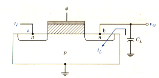
Using an NMOS transmission gate in a MOS circuit may introduce a dynamic condition. [link] shows a cross-section of the NMOS transistor in the transmission gate configuration. If , then the load capacitor charges to . When , the NMOS device turns off and the input and output become isolated.
The capacitor voltage reverse biases the pn junction between terminal b and ground. A reverse-biased pn junction leakage current begins to discharge the capacitor, and the circuit does not remain in a static condition. This circuit is now dynamic in that the high output does not remain constant with time.
CMOS Transmission Gate
A CMOS transmission gate is shown in [link]a. The parallel combination of NMOS and PMOS transistors, with complementary gate signals, allows the input signal to be transmitted to the output without the threshold voltage attenuation. Both transistors must be bilateral, therefore, the NMOS substrate is connected to the most negative potential in the circuit and the PMOS substrate is connected to the most positive potential (usually, ground and , respectively). [link]b shows a frequently used simplified circuit symbol for the CMOS transmission gate.
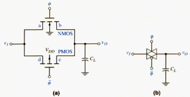
We again assume that the transmission gate is to operate over a voltage range of zero-to- . If the control voltages are and , then both the NMOS and PMOS transistors are cut off and the output is isolated from the input. In this state, the circuit is essentially an open switch.
If , , , and is initially zero, then for the NMOS device, terminal a acts as the drain and terminal b acts as the source, whereas for the PMOS device, terminal c acts as the drain and terminal d acts as the source. Current enters the NMOS drain and the PMOS the PMOS source, as shown in [link]a, to charge the load capacitor. The NMOS gate-to-source voltage is
and the PMOS source-to-gate voltage is
As with the NMOS transmission gate, when , the NMOS transistor cuts off and since . However, since the source-to-gate voltage of the PMOS device is constant at , the PMOS transistor continues to conduct. The drain current iDP goes to zero when the PMOS source-to-drain voltage goes to zero, or . This means that the load capacitor continues to charge through the PMOS device until the output and input voltages are equal, or in this case, .
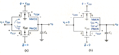
Consider what happens if , and initially. For the NMOS device, terminal a acts as the source and terminal b acts as the drain, whereas for the PMOS device, terminal c acts as source and terminal d acts as the drain. Current enters the NMOS drain and the PMOS source, as shown in [link]b, to discharge the capacitor. The NMOS gate-to-source voltage is
and the PMOS source-to-gate voltage is
When , the PMOS device cuts off and goes to zero. However, since , the NMOS transistor continues conducting and capacitor completely discharges to zero.
Using a CMOS transmission gate in a MOS circuit may introduce a dynamic condition. [link] shows the CMOS transmission gate with simplified cross sections of the NMOS and PMOS transistors. If = 0 and , then the input and output are isolated. If , then the NMOS substrate-to-terminal b pn junction is reverse biased and capacitance can discharge, as it did in the NMOS transmission gate. If, however, = 0, then the PMOS terminal c-to-substrate pn junction is reversed bias and capacitance can charge to a positive voltage. This circuit is therefore dynamic in that the output high or low conditions do not remain constant with time.
CMOS Pass Networks
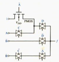
CMOS transmission gate may also be used in pass network logic design. CMOS pass networks use NMOS transistors to pass 0’s, PMOS transistors to pass 1’s and CMOS transmission gates to pass a variable to the output. An example is shown in [link]. One PMOS transistor is used to transmit a logic 1, while transmission gates are used to transmit a variable that may be either a logic 1 or a logic 0. We can show that for any combination of signals, a logic 1 or logic 0 is definitely passed to the output.
SHIFT REGISTER AND FLIP-FLOPS
In the logic circuits previously considered such as NOR or NAND logic gates, the output is directly related to the input by some logic combination. The circuits are therefore classified as combinational logic circuits.
Another class of circuits is called sequential logic circuits. The output depends not only on the inputs, but also on the previous values of the inputs. Shift registers and flip-flops are typical examples of such circuits. Sequential logic circuits have digital memory. These circuits usually store information for a short time until that information is transferred to another part of the system.
In this section, we introduce a basic shift register and the basic concept with logic diagrams. Additional information can be found in more advanced texts.
Dynamic Shift Registers
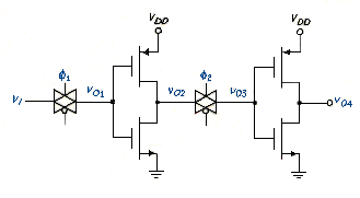
A shift register can be formed using transmission gates and inverters. [link] shows a combination of NMOS transmission gates and NMOS depletion-load inverters. The clock signals applied to the gates of the NMOS transmission gates must be complementary, nonoverlapping pulses. The effective capacitances at the gates of MD1 and MD2 are indicated by the dotted connections to CG1 and CG2.
If, for example, CG1 is initially uncharged when and if when , then a logic 1 = voltage should exist at at the end of clock pulse . The capacitance charges through , and the driving circuit of . The effective R-C time constant must be sufficiently small to achieve this charging effect. As goes high, goes low, but the low is not transmitted through as long as remains low.
[link] is used to determine the operation of this circuit and the voltages at various times. For simplicity, we assume that = 5 V and = 1 V for the NMOS drivers and transmission gate transistors.
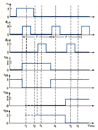
At t = , , charges to , and goes low. At this time, is still cut off, which means that the values of and depend on the previous history. At t = , is zero, is cut off, but remains charged. At t = , is high, and the logic 0 at is transmitted to , which forces to 5 V. The input signal = 5 V at t = has thus been transmitted, or shifted, from the input to the output during one clock cycle, making this circuit one stage of a shift register.
At t = , = 0, and = 5V, so that = 0 and = 5 V. Since = 0, MN2 is cut off, and and are isolated. At t = , = 5 V, so that charges to , and goes low (logic 0). At t = , both NMOS transmission gates are cut off, and the two inverters remain in their previous states. It is important that and do not overlap, or the signal would propagate through the whole chain at once and we would no longer have a shift register.
In the dynamic condition of NMOS transmission gates the high output voltage across the output capacitance does not remain constant with time; it discharges through the transmission gate transistor. This same effect applies to the shift register shown in [link]. For example, from [link], at t = , = 4 V, = 0, and is cut off. Voltage v01 will start to decay and v02 will begin to increase. To prevent logic errors from being introduced into the system, the clock signal period T must be small compared to the effective R-C discharge time constant. The circuit shown in [link] is therefore called a dynamic shift register.
A dynamic shift register formed in a CMOS technology is shown in [link]. Operation of this circuit is very similar to the dynamic NMOS shift register, except for the voltage levels. For example, when , then and . When goes high, then goes to zero, , and the input signal is shifted to the output during one clock period.
R-S Flip-Flop
Flip-flops are bistable circuits usually formed by cross-coupling two NOR gates. [link] shown an R-S flip-flop using NMOS NOR logic gates with depletion loads. As shown, , , and form one NOR gate, and , , and form the second. The outputs of the two NOR circuits are connected back to the inputs of the opposite NOR gates.
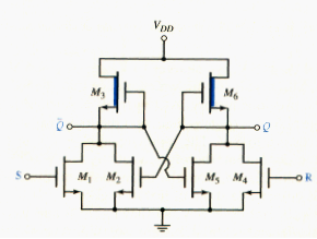
If we assume that S = logic 1 and R = logic 0, then is biased in its conducting state and output is forced low. The inputs to both and are low, so output goes high to a logic 1 = . Transistor is then also biased in a conducting state. The two outputs Q and are complementary and, by definition, the flip-flop is in the set state when Q = logic 1 and logic 0.
If S returns to logic 0, then turns off, but remains turned on so remains low and Q remains high. Therefore, when S goes low, nothing in the circuit can force a change and the flip-flop stores this particular logic state.
If both S and R inputs were to go high, then both outputs Q and would go low. However, this would mean that the output would be complementary. Therefore, a logic 1 at both S and R is considered to be a forbidden or nonallowed condition. If both inputs go low simultaneously, then the outputs will flip into one state or the other, as determined by slight imbalances in transistor characteristics.
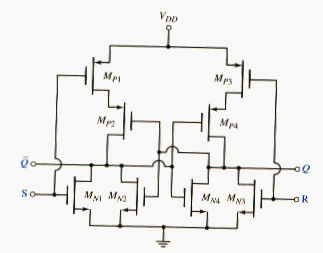
[link] shows an R-S flip-flop using CMOS NOR logic gates. The outputs of the two NOR gates are connected back to the inputs of the opposite NOR gate to form the flip-flop.
If S = logic 1 and R = logic 0, then is turned o, is cut off, and goes low. With = R = logic 0, then both and are cut off, both and are biased in a conducting state so that the output Q goes high. With Q = logic 1, is biased on, is biased off, and the flip-flop is in a set condition. When S goes low, turns off, but remains conducting so the state of the flip-flop does not change.
When S = logic 0 and R = logic 1, then output Q is forced low, output goes high, and the flip-flop is in a reset condition. Again, a logic 1 at both S and R is considered to be a forbidden or a nonallowed condition, since the resulting outputs are not complementary.
D Flip-Flop
A D-type flip-flop is used to provide a delay. The logic bit on D input is transferred to the output at the next clock pulse. This flip-flop is used in counters and shift registers. The basic circuit is similar to the CMOS dynamic shift register shown in [link], except that additional circuitry makes the D flip-flop a static circuit.
Consider the circuit shown in [link]. The CMOS inverter composed of and is driven by a CMOS transmission gate composed of and . A second CMOS inverter, and , is connected in a feedback configuration. If = high, then goes high when the transmission gate is conducting, and output v0, which is the input to the feedback inverter, goes low.
When the CMOS transmission gate turns off, the pn junction in the transmission gate transistor is reverse biased. In this case, however, voltage is not simply across the gate capacitance of inverter - . Transistor is biased in a conducting state, so the reverse-biased pn junction leakage current is supplied through , as indicated in [link]. Since this leakage current is small, the source-to-drain voltage of will be small, and will remain biased at essentially VDD. The circuit will therefore remain in this static condition.
Similarly, when is low and is high, the pn junction in the transmission gate transistor is reverse-biased and transistor is biased on. Transistor sinks the pn junction leakage current , and the circuit remains in this static condition until charged by a new input signal through the transmission gate.
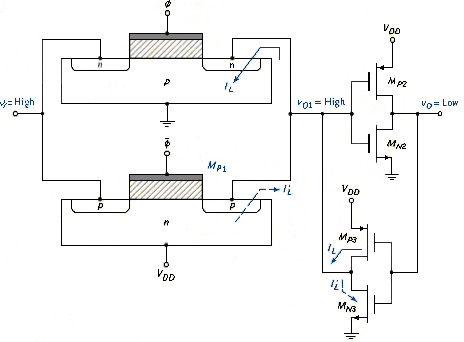
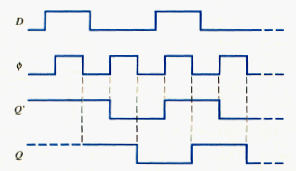
The circuit shown in [link] is a master-slave configuration of a D flip-flop. When clock pulse is high, transmission gate TG1 is conducting and data D goes through the first inverter, which means that . Transmission gate TG2 is off, so data stops at Q’. When clock pulse goes low, then TG3 turns on, and the master portion of flip-flop is a static configuration. Also when goes low, TG2 turns on, the data are transmitted through the slave portion of the flip-flop, and the output is Q = = D. the data present when is high are transmitted to the output of the flip-flop during the negative transition of the clock pulse. The various signals in the D flip-flop are shown in [link].
Additional circuitry can be added to the D flip-flop shown in [link] to provide a set and reset capability.

SUMMARY
In this chapter, NMOS and CMOS digital logic circuit were analyzed and designed. Basic NMOS and CMOS logic gates, and examples of shift registers and flip-flops were discussed. We also analyzed NMOS and CMOS transmission gates.
The NMOS inverter is the basic of NMOS logic circuits. We generated the voltage transfer characteristics of NMOS inverters with various load devices.
The CMOS inverter is the basis of CMOS logic circuits. We generated the voltage transfer characteristics of the CMOS inverter. For the CMOS circuit, quiescent power dissipation is essentially zero when the input is in either logic state; power is dissipated only when the output is switching logic states. Even with a switching frequency on the order of 1 MHz, the power dissipation in a CMOS inverter can be at least an order of magnitude less than that in an NMOS inverter. This is the principal advantage of CMOS logic circuits.
We than analyzed classical CMOS NOR and NAND gates. Since PMOS devices must be approximately twice as large as NMOS devices to produce equivalent conduction parameters, a large saving in chip area can be realized by eliminating as many PMOS transistors as possible. Clocked CMOS logic circuits achieve this goal. A generalized NMOS logic circuit is inserted between a PMOS and NMOS device. The power dissipation advantage of CMOS is thus maintained.
Transmission gates are used as switches and can steer logic signals through a digital system. We analyzed both NMOS and CMOS transmission gates. These transmission gates can also be used to form logic circuits.
Dynamic shift registers are formed by connecting two inverters through transmission gates. We analyzed examples of both NMOS and CMOS dynamic shift registers, as well as NMOS and CMOS R-S flip-flops. An R-S flip-flop is formed by cross-coupling the inputs and outputs of two NOR logic gates. Finally, we discussed a CMOS D-type flip-flop.