INTRODUCTION
Having understood the fundamental laws of circuit theory (Ohm’s law and Kirchhhoff’s laws), we are now prepared to apply to develop two powerful techniques for circuit analysis: nodal analysis, which is based on a systematic application of Kirchhoff’s current law (KCL) and mesh analysis which based on a systematic application of Kirchhoff’s voltage law (KVL). The two techniques are so important that this chapter should be regarded as the most important in the book. Students are therefore encouraged to pay careful attention.
With the two techniques to be developed in this chapter we can analyze any linear circuit by obtaining a set of simultaneous equation that are then solved to obtain the required values of current or voltage. One method of solving simultaneous equations involves Cramer’s rule, which allow us to calculate circuit variables as a quotient of determinants.
Finally, we apply the technique learned in this chapter to analyze transistor circuits.
NODAL ANALYSIS
Nodal analysis provides a general procedure circuits using node voltages as the circuit variables. Choosing node voltages instead of element voltages as circuit variables is convenient and reduces the number of equations one must solve simultaneously.
To simplify matters, we shall assume in this section that circuits do not contain voltage sources. Circuits that contain voltage sources will be analyzed in the next section.
In nodal analysis, we are interested in finding the node voltages. Given a circuit with n nods without voltage sources, the nodal analysis of the circuit involves taking the following three steps.
Steps to determine node voltages:
- Select a node as the reference node. Assign voltages , , …, to remaining n – 1 nodes. The voltages are referenced with respect to the reference node.
2. Apply KCL to each of the n-1 nonreference nodes. Use Ohm’s law to express the branch currents in term of node voltages.
3. Solve the resulting simultaneous equations to obtain the unknown node voltages.
We shall now explain and apply these three steps.
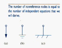
The first step in nodal analysis is selecting a node as the reference or datum node. The reference node is commonly called the ground since it is assumed to have zero potential. A reference node is indicated by any of the three symbols in [link]. The type of ground in [link](b) is called a chassis ground and is used in devices where the case, enclosure, or chassis acts as reference point for all circuits. When the potential of the earth is used as reference, we use the earth ground in [link](a) or [link](c). We shall always use the symbol in [link](b).
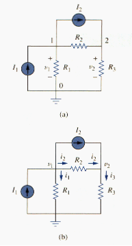
Once we have selected a reference node, we assign voltage designations to nonreference nodes. Consider, for example, the circuit in [link](a). Node 0 is the reference node (v = 0), while nodes 1 and 2 are assigned voltages and , respectively. Keep in mind that the node voltages are defined with respect to the reference node. As illustrated in [link](a) each node voltage is the voltage rise from the reference node to the corresponding nonreference node or simply the voltage of that node with respect to the reference node.
As the second step, we apply KCL to each nonreference node in the circuit. To avoid putting too much information on the same circuit, the circuit in [link](a) is redrawn in [link](b), where we now add , , and as the circuits through resistors , , and , respectively. At node 1, applying KCL gives
At node 2,
We now apply Ohm’s to express the unknown currents , , and in term of node voltages. The key idea to bear in mind is that, since resistance is a passive element, by the passive sign convention, current must always flow from a higher potential to a lower potential.
Current flows from a higher potential to a lower potential in a resistor.
We can express this principle as
Note that this principle is in agreement with the way we define resistance in chapter 2 (see Figure 2.1). With this in mind, we obtain from [link](b),
or
or
or
Substituting [link] in [link] and [link] results, respectively, in
In terms of the conductances, [link] and [link] become
The third step in nodal analysis is to solve for the node voltages. If we apply KCL to n-1 nonreference nodes, we obtain n-1 simultaneous equations such as [link] and [link] or [link] and [link]. For the circuit of [link], we solve [link] and [link] or [link] and [link] to obtain the node voltages and using any standard method, such as substitution method, elimination method, Cramer’s rule or matrix inversion. To use either of the last two methods, one must cast the simultaneous equations in matrix form. For example, [link] and [link] can be cast in matrix form as
which can be solved to get and . [link] will be generalized in section 6. The simultaneous equations may also be solved using calculator or with software package such as MATLAB.
NODAL ANALYSIS WITH VOLTAGE SOURCES
We now consider how voltage sources effect nodal analysis. We use the circuit in [link] for illustration. Consider the following two possibilities.
CASE 1: if a voltage source is connected between the reference node and a nonreference node, we supply set the voltage at the nonreference node equal to the voltage of the voltage source. In [link], for example,
Thus our analysis is somewhat simplified by this knowledge of the voltage at this node.
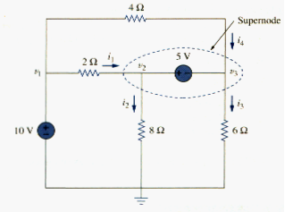
CASE 2: If the voltage source (dependent or independent) is connected between two nonreference nodes, the two nonreference nodes form a generalized node or supernode; we apply both KCL and KVL to determine the node voltages.
A supernode is formed by enclosing a (dependent or independent) voltage source connected between two nonreference nodes and any elements connected in parallel with it.
In [link], nodes 2 and 3 form a supernode. We analyze a circuit with supernode using the same three steps mentioned in the previous section except that the supernodes are treated differently. Why? Because an essential component of nodal analysis is applying KCL, which requires knowing the current through each element. There is no way of knowing the current through a voltage source in advance. However, KCL must be satisfied at a supernode like any other node. Hence, at the supernode in [link],
or
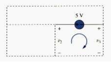
To apply Kirchhoff’s voltage law to the supernode in [link], we redraw the circuit as shown in [link]. Going around the loop in the clockwise direction gives
From [link], [link] and [link], we obtain the node voltages.
Note the following properties of a supernode:
1. The voltage source inside the supernode provides a constraint equation needed to solve for the node voltage.
2. A supernode has no voltage of it own.
3. A supernode requires the application of both KCL and KVL.
MESH ANALYSIS
Mesh analysis is also known as loop analysis or the mesh current method. Mesh analysis provides another general procedure for analyzing circuits using mesh currents as the circuit variables. Using mesh currents instead of element currents as circuit variables is convenient and reduces the number of equations that must be solved simultaneously. Recall that a loop is closed path with no node passed more than once. A mesh is a loop that does not contain any other loop within it.
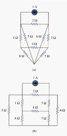
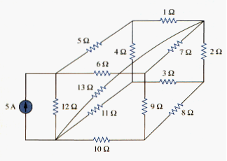
Nodal analysis applies KCL to find unknown voltages in a given circuit, while mesh analysis applies KVL to find unknown currents. Mesh analysis is not quite as general as nodal analysis because it is only applicable to a circuit that is planar. A planar circuit is one that can be drawn in a plane with no branches crossing one another; otherwise it is nonplanar. A circuit may have crossing branches and still be planar if it can be redrawn such that it has no crossing branches. For example, the circuit in [link](a) has two crossing branches, but it can be redrawn as in [link](b). Hence, the circuit in [link](a) is planar. However, the circuit in [link] is nonplanar, because there is no way to redraw it and avoid the branches crossing. Nonplanar circuits can be handled using mesh analysis, but they will not be considered in this text.
To understand mesh analysis, we should first explain more about what we mean by a mesh.
A mesh is a loop which does not contain any other loop within it.
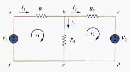
In [link], for example, paths abefa and bcdeb are meshes, but path abcdefa is not a mesh. The current through a mesh is known as mesh current. In mesh analysis, we are interested in applying KVL to find the mesh currents in a given circuit.
In this section, we will apply mesh analysis to planar circuits that do not contain current sources. In the next section, we will consider circuits with current sources. In the mesh analysis of a circuit with n meshes, we take the following three steps.
Steps to determine mesh currents:
- Assign mesh currents , , …, in to the n mesh.
- Apply KVL to each of n meshes. Use Ohm’s law to express the voltages in term of the mesh currents.
- So the resulting n simultaneous equations to get the mesh currents.
To illustrate the steps, consider the circuit in [link]. The first step requires that mesh currents and are assigned to meshes 1 and 2. Although a mesh current may be assigned to each mesh in arbitrary direction, it is conventional to assume that each mesh current flows clockwise.
As the second step, we apply KVL to each mesh. Applying KVL to mesh 1, we obtain
Or
For mesh 2, applying KVL gives
or
The third step is to solve for the mesh currents. Putting [link] and [link] in matrix form yields
Notice that the branch currents are different from the mesh current unless the mesh is isolated. To distinguish between the two types of currents, we use i for a mesh current and I for a branch current. The current elements , , and are algebraic sums of the mesh currents. It is evident from [link] that
,
MESH ANALYSIS WITH CURRENT SORCES
Applying mesh analysis to circuits containing current sources (dependent or independent) may appear complicated. But it is actually much easier than what we encountered in the previous section, because the presence of the current sources reduces the number of equations. Consider the following two possible cases.
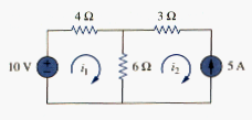
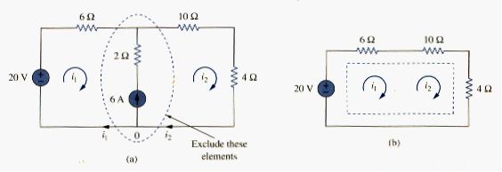
CASE 1. When a current source exists only in one mesh: consider the circuit in [link], for example. We set and write a mesh equation for the other mesh in the usual way, that is,
CASE 2. When a current source exists between two meshes: consider the circuit in [link](a), for example. We create a supermesh by excluding the current source and any elements connected in series with it, as shown in [link](b). Thus,
A supermesh results when two meshes have a (dependent or independent) current source in common.
As shown in [link](b), we create a supermesh as the periphery of the two meshes and treat it differently. If a circuit has two or more supermeshes that intersect, they should be combined to form a larger supermesh. Why treat the supermesh differently? Because mesh analysis applies KVL-which requires that we know the voltage across each branch-and we do not know the voltage across a current source in advance. However, a supermesh must satisfy KVL like any other mesh. Therefore, applying KVL to the supermesh in [link](b) gives
or
We apply KCL to a node in the branch where the two meshes intersect. Applying KCL to node 0 in [link](a) gives
Solving [link] and [link], we get
and
Note the following properties of a supermesh:
1. The current source in the supermesh provides the constraint equation necessary to solve for the mesh currents.
2. A supermesh has no current of its own.
3. A supermesh requires the application of both KVL and KCL.
NODAL AND MESH ANALYSIS BY INSPECTION
This section presents a generalized procedure for nodal or mesh analysis. It is a shortcut approach based on mere inspection of a circuit.
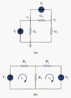
When all sources in a circuit are independent current sources, we do not need to apply KCL to each node to obtain the node-voltage equations as we did in section 2. We can obtain the equations by mere inspection of the circuit. As an example, let us reexamine , shown again in [link](a) for convenience. The circuit has two nonreference nodes and the node equations were derived in section 2 as
Observe that each of the diagonal terms is sum of the conductances connected directly to node 1 or 2, while the off-diagonal terms are the negatives of the conductances connected between the nodes. Also, each term on the right-hand side of [link] is the algebraic sum of the currents entering the node.
In general, if a circuit with independent current sources has N nonreference nodes, the node-voltage equations can be written in term of the conductances as
or simply
where
= Sum of the conductances connected to node k
= = negative of the sum of the conductances directly connecting nodes k and j,
= Unknown voltage at node k
= Sum of all independent current sources directly connected to node k, with currents entering the node treated as positive
G is called the conductance matrix: v is the output vector; and i is the input vector. [link] can be solved to obtain the unknown node voltages. Keep in mind that is valid for circuits only independent current sources and linear resistors.
Similarly, we can obtain mesh-current equations by inspection when a linear resistive circuit has only independent voltage sources. Consider the circuit in [link](b) for convenience. The circuit has two nonreference nodes and the node equations were derived in Section 4 as
We notice that each of the diagonal terms is the sum of the resistances in the related mesh, while each of the off-diagonal terms is the negative of the resistance common to meshes 1 and 2. Each term on the right-hand side of [link] is the algebraic sum taken clockwise of all independent voltage sources in the related mesh.
In general, if the circuit has N meshes, the mesh-current equations can be expressed in terms of the resistances as
or simply
where
= Sum of the resistances in mesh k
= = negative of the sum of the resistances in common with meshes k and j,
= Unknown current for mesh k in the clockwise direction
= Sum taken clockwise of all independent voltage sources in mesh k, with voltage rise treated as positive
R is called the resistance matrix: v is the output vector; and i is the output vector; and v is the input vector. We can solve [link] to obtain the unknown mesh currents.
NODAL VERSUS MESH ANALYSIS
Both nodal and mesh analyses provide a systematic way of analyzing a complex network. Someone may ask: given a network to be analyzed, how do we know which method is better or more efficient? The choice of the better method is dictated by two factors.
The first factor is the nature of the particular network. Networks that contain many series-connected elements, voltage sources, or supermeshes are more suitable for mesh analysis, whereas networks with parallel-connected elements, current sources or supernodes are more suitable for nodal analysis. Also, circuit with fewer nodes than meshes is better analyzed using nodal analysis, while a circuit with fewer meshes than nodes is better analyzed using mesh analysis. The key is to select the method that results in the smaller number of equations.
The second factor is the information required. If node voltages are required, it may be expedient to apply nodal analysis. If branch or mesh currents are required, it may be better to use mesh analysis.
It is helpful to be familiar with both methods of analysis, for at least two reasons. First, one method can be used to check the results from the other method, if possible. Second, since each method has its limitations, only one method may be suitable for a particular problem. For example, mesh analysis is the only method to use in analyzing transistor circuits, as we shall see in section 8. But mesh analysis cannot easily be used to solve an op amp circuit, as we shall see in chapter 5, because there is no direct way to obtain the voltage across the op amp itself. For nonplanar networks, nodal analysis is the only option, because mesh analysis only applies to planar networks. Also, nodal analysis is more amenable to solution by computer, as it is easy to program.
APPLICATIONS: DC TRANSISTOR CIRCUITS
Most of us deal with electronic products on a routine basis and have some experience with personal computers. A basic component for the integrated circuits found in these electronics and computers is the active, three terminal device known as the transistor. Understanding the transistor is essential before an engineer can start an electronic circuit design.
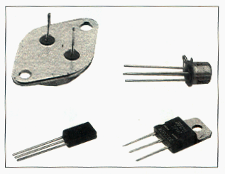
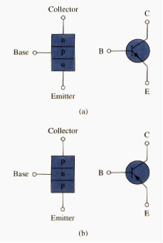
[link] depicts various kinds of transistors commercially available. There are two basic types of transistors: bipolar junction transistors (BJTs) and field-effect transistor (FETs). Here, we consider only the BJTs, which were the first of the two and are still used today. Our objective is to present enough detail about the BJT to enable us to apply the techniques developed in this chapter to analyze dc transistor circuits.
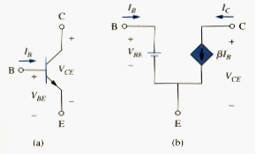
There two types of BJTs: npn and pnp, with their circuit symbols as shown in [link]. Each type has three terminals, designated as emitter (E), base (B), and collector (C). For the npn transistor, the currents and voltages of the transistor are specified as in [link]. Applying KCL to [link](a) gives
where , , and are emitter, collector, and base currents, respectively.
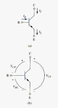
Similarly, applying KVL to [link](b) gives
Where , , and are collector-emitter, emitter-base, and base-collector voltages. The BJT can operate in one of three modes: active, cutoff, and saturation. When transistors operate in the active mode, typically ,
Where is called the common-base current gain. In [link], denotes the fraction of electrons injected by the emitter that are colleted by the collector. Also,
Where is known as the common-emitter current gain. The and are characteristic properties of a given transistor and assume constant values for that transistor. Typically, takes values in the range of 0.98 to 0.999, while takes values in the range 50 to 1000 from [link] to [link], it is evident that
and
These equations show that, in the active mode, the BJT can be modeled as a dependent current-controlled current source. Thus, in circuit analysis, the dc equivalent model in [link](b) may be used to replace the npn transistor in [link](a). Since in [link] is large, a small base current controls large currents in the output circuit. Consequently, the bipolar transistor can be serve as an amplifier, producing both current gain and voltage gain. Such amplifiers can be used to furnish a considerable amount of power to transducers such as loudspeakers or control motors.
It should be observed in the following examples that one cannot directly analyze transistor circuits using nodal analysis because of the potential difference between the terminals of the transistor. Only when the transistor is replaced by its equivalent model, we can apply nodal analysis.
SUMMARY
- Nodal analysis is the application of Kirchhoff’s current law at the nonreference nodes. It is applicable to both planar and nonplanar circuits. We express the result in terms of the node voltage. Solving the simultaneous equations yields the node voltages.
- A supernode consists of two nonreference nodes connected by a (dependent or independent) voltage source.
- Mesh analysis is the application of Kirchhoff’s voltage law around meshes in a planar circuit. We express the result in term of mesh currents. Solving the simultaneous equations yields the mesh currents.
- A supermesh consists of two meshes that have a (dependent or independent) current source in common.
- Nodal analysis is normally used when a circuit has fewer node equations than mesh equations. Mesh analysis is normally used when circuit has fewer mesh equations than node equations.
- DC transistor circuits can be analyzed using the techniques covered in this chapter.