INTRODUCTION
Having learned the basic laws and theorems for circuit analysis, we are now ready to study an active circuit element of paramount importance: the operational amplifier or op amp for short. The op amp is a versatile circuit building block.
The op amp is an electronic unit that behaves like a voltage-controlled voltage source.
It can also be used in making a voltage or current controlled current source. An op amp can sum signal, amplify signal, integrate it, or differentiate it. The ability of the op amp to perform these mathematical operations is the reason it is called an operational amplifier. It is also the reason for the widespread use of op amps in analog design. Op amps are popular in practical circuit designs because they are versatile, inexpensive, ease to use, and fun to work with.
We begin by discussing the ideal op amp and later consider the nonideal op amp. Using nodal analysis as a tool, we consider ideal op amp circuits such as the inverter, voltage follower, summer, and difference amplifier. Finally, we learn an op amp is used in digital-to-analog converters and instrumentation amplifiers.
OPERATIONAL AMPLIFIERS
An operational amplifier is designed so that it performs some mathematical operations when external components, such as resistors and capacitors, are connected to its terminals. Thus,
An op amp is an active circuit element designed to perform mathematical operations of addition, substraction, multiplication, division, differentiation, and integration.
The op amp is an electronic device consisting of a complex arrangement of resistors, transistors, capacitors, and diodes. A full discussion of what is inside the op amp is beyond the scope of this block. It will suffice to treat the op amp as a circuit building block and simply study what takes place at its terminals.
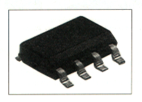
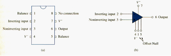
Op amps are commercially available in integrated circuit packages in several forms. [link] shows a typical op amp package. A typical one is the eight-pin dual in-line package (or DIP), shown in [link](a). Pin or terminal 8 is unused, and terminals 1 and 5 are of little concern to us. The five important terminals are:
1. The inverting input, pin 2,
2. The noninverting input, pin 3,
3. The output, pin 6,
4. The positive power supply , pin 7,
5. The negative power supply , pin 4.
The circuit symbol for the op amp is the triangle in [link](b); as shown, the op amp has two inputs and one output. The inputs are marked with minus (-) and plus (+) to specify inverting and noninverting inputs, respectively. An input applied to the to the noninverting terminal will appear with the same polarity at the output, while an input applied to the inverting terminal will appear inverted at the output.
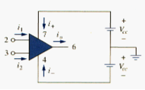
As an active element, the op amp must be powered by a voltage supply as typically show in [link]. Although the power supplies are often ignored in op amp circuit diagrams for the sake of simplicity, the power supply currents must not be overlooked. By KCL,
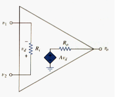
The equivalent circuit model of an op amp is shown in [link]. The output section consists of a voltage-controlled source in series with the output resistance R0. It is evident from [link] that the input resistance g, is the Thevenin equivalent resistance seen at the input terminals, while the output resistance is the Thevenin equivalent resistance seen at the output. The differential input voltage is given by
Where is the voltage between the inverting terminal and ground and is the voltage between the noninverting terminal and ground. The op amp senses the difference between the two inputs, multiplies it by the gain A, and cause the resulting voltage to appear at the output. Thus, the output is given by
A is called the open-loop voltage gain because it is the gain of the op amp without any external feedback from output to input. [link] shows typical values of voltage gain A, input resistance , output resistance , and supply voltage .
| Parameter | Typical range | Ideal values |
| Open loop gain, A | to | |
| Input resistance, | to | |
| Output resistance, | 10 to 100 | |
| Supply voltage, | 5 to 24 V |
The concept of feedback is crucial to our understanding of op amp circuits. A negative feedback is achieved when the output is fed back to the inverting terminal of the op amp. When there is a feedback path from output to input of the op amp, the ratio of the output voltage to the input voltage is called the closed loop gain. As a result of the negative feedback, it can be shown that the closed-loop gain is almost insensitive to the open-loop gain A of the op amp. For this reason, op amps are used in circuit with feedback paths.
A practical limitation of the op amp is that the magnitude of its output voltage cannot exceed . In other words, the output voltage is dependent on and is limited by the power supply voltage. [link] illustrates that the op amp can operate in three modes, depending on the differential input voltage :
1. Positive saturation, ,
2. Linear region, ,
3. Negative saturation, .
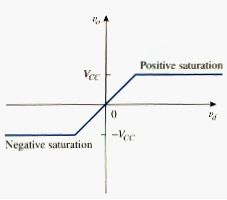
Although we shall always operate the op amp in the linear region, the possibility of saturation must be borne in mind when one design with op amps, to avoid designing op amp circuits that will not work in the laboratory.
IDEAL OPERATIONAL AMPLIFIERS
To facilitate the understanding of op amp circuits, we will assume ideal op amp. An op amp is ideal if it has the following characteristics:
- Infinite open loop gain, ,
- Infinite input resistance, ,
- Zero output resistance, .
An ideal op amp is an amplifier with infinite open-loop gain, infinite input resistance and zero output resistance.
Although assuming an ideal op amp provides only approximate analysis, most modern amplifiers have such large gain and input impedance that the approximate analysis is a good one. Unless stated otherwise, we will assume from now on that every op amp is ideal.
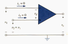
For circuit analysis, the ideal op amp is illustrated in [link], which is derived from the nonideal model in [link]. Two important characteristics of the op amp are:
1. The current into both input terminals are zero:
and
This is due to infinite input resistance. An infinite resistance between the input terminals implies that an open circuit exists there and current cannot enter the op amp. But the output circuit is not necessary zero according to [link].
2. The voltage across the input terminals is negligibly small; i.e.,
Or
Thus, an ideal op amp has zero current into its two input terminals and negligibly small voltage between the two input terminals. [link] and [link] are extremely important and should be regarded as the key handles to analyzing op amp circuits.
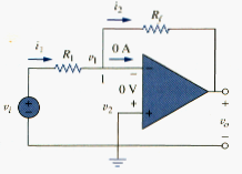
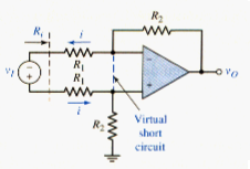
INVERTING AMPLIFIER
In this and following sections, we consider some useful op amp circuits that often serve as modules for designing more complex circuits. The first of such op amp circuits is the inverting amplifier shown in [link]. In this circuit, the noninverting circuit is grounded. vi is connected to the inverting input through , and the feedback resistor is connected between the inverting input and output. Our goal is to obtain the relationship the input voltage vi and the output voltage v0. Applying KCL at node 1,
But for an ideal op amp, since the noninverting terminal is grounded. Hence,
Or
The voltage gain is . The designation of the circuit in [link] as an inverter arises from the negative sign. Thus,
An inverting amplifier reverses the polarity of the input signal while amplifying it.
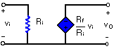
Note that the gain is the feedback resistance divided by the input resistance which means that the gain depends only on the external elements connected to the op amp. In view of [link], an equivalent circuit for the inverting amplifier is shown in [link]. The inverting amplifier is used, for example, in current to voltage converter.
NONINVERTING AMPLIFIER
Another important application of the op amp is the noninverting amplifier shown in [link]. In this case, the input voltage is applied directly at the noninverting input terminal and resistor is connected between ground and the inverting terminal. We are interested in the output voltage and the voltage gain. Application of KCL at the inverting terminal gives
But . [link] becomes
Or
The voltage gain is , which does not have a negative sign. Thus, the output has the same polarity as the input.
A noninverting amplifier is an op amp circuit designed to provide a positive voltage gain.
Again we notice that the gain depends only on the external resistors.
Notice that if feedback resistor (short circuit) or (open circuit) or both, the gain becomes 1. Under these conditions ( and ), the circuit in [link] becomes that shown in [link], which is called a voltage follower (or unity gain amplifier) because the output follows the input. Thus, for a voltage follower
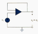
Such circuit has very high input impedance and is therefore useful as an intermediate-stage (or buffer) amplifier to isolate one circuit from another as portrayed in [link]. The voltage follower minimizes interaction between the two stages and eliminates interstage loading.
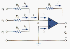
SUMMING AMPLIFIER
Besides amplification, the op amp can perform addition and subtraction. The addition is performed by the summing amplifier covered in this section; the subtraction is performed by the difference amplifier covered in the next section.
A summing amplifier is an op amp circuit that several inputs and produce an output that is the weighted sum of the inputs.
The summing amplifier, shown in [link], is variation of the inverting amplifier. It takes advantage of the fact that the inverting configuration can handle many inputs at the same time. We keep in mind that the current entering each op amp input is zero. Applying KCL at node a gives
But
We note that and substitute [link] into [link]. We get
Indicating that the output voltage is a weighted sum of the inputs. For this reason, the circuit in [link] is called a summer. Needless to say, the summer can have more than three inputs.
DIFFERENCE AMPLIFIER
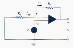
Difference (or differential) amplifiers are used in various applications where there is need to amplify the difference between two input signals. They are first cousins of the instrumentation amplifier, the most useful and popular amplifier, which we will discuss in section 9.
A difference amplifier is a device that amplifies the difference between two inputs but rejects any signals common to the two inputs.
Consider the op amp circuit shown in [link]. Keep in mind that zero currents enter the op amp terminals. Applying KCL to node a,
or
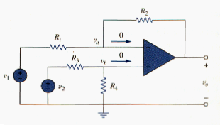
Applying KCL to node b,
Or
but . Substituting [link] into [link] yields
Or
Since a difference amplifier must reject a signal common to the two inputs, the amplifier must have the property that when . This property exists when
Thus, when the op amp circuit is a difference amplifier, [link] becomes
Which indicated that this amplifier has a differential gain of . This factor is a closed-loop differential gain.
If and , the difference amplifier becomes a substractor, with the output
As previously stated, another important characteristic of electronic circuits is the input resistance. The differential input resistance of the differential amplifier can be determined using the circuit shown in [link]. In the Figure, we have imposed the condition given in [link] and have set and . The input resistance is then defined as
Taking into account the virtual short concept, we can write a loop equation, as follows:
Therefore, the input resistance is
In the ideal difference amplifier, the output v0 is zero when . However, an inspection of [link] shows that this condition is not satisfied if . When , the input is called a common mode input signal. The common mode input voltage is defined as
The common mode gain is then defined as
Ideally, when a common mode signal is applied, and .
A nonzero common mode gain may be generated in actual op-amp circuits. A figure of merit for a difference amplifier is the common mode rejection ratio (CMRR), which is defined as the amplitude of the ratio of differential gain to common mode gain, or
Usually, the CMRR is expressed in decibels, as follows:
Ideally, the common mode rejection ratio is infinite. In an actual differential amplifier, we would like the common mode rejection ratio to be as large as possible.
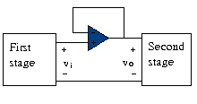
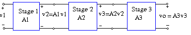
CASCADED OP AMP CIRCUITS
As we know, op amp circuits are modules or building blocks for designing complex circuits. It is necessary in practical applications to connect op amp circuits in cascade (i.e. head to tail) to achieve a large overall gain. In general, two circuits are cascaded when they are connected in tandem, one behind another in a single file.
A cascade connection is a head to tail arrangement of two or more op amp circuits such that the output of one is the input of the next.
When op amp circuits are cascaded, each circuit in the string is called a stage; one original input signal is increased by the gain of the individual stage. Op amp circuits have the advantage that they can be cascaded without changing their input-output relationships. This is due to the fact that each (ideal) op amp circuit has infinite input resistance and zero output resistance. [link] displays a block diagram representation of three op amp circuits in cascade. Since the output of one stage is the input to the next stage, the overall gain of the cascade connection is the product of the gain of the individual op amp circuits, or
Although the cascade connection does not effect the op amp input-output relationships, care must be exercised in the design of an actual op amp circuit to ensure that the load due to the next stage in the cascade does not saturate the op amp.
APPLICATIONS
The op amp is a fundamental building block in modern electronic instrumentation. It is used extensively in many devices, along with resistors and other passive elements. Its numerous practical applications include instrumentation amplifiers, digital to analog converters, analog computers, level shifters, filters, calibration circuits, inverters, summers, integrators, differentiators, substractors, logarithmic amplifiers, comparators, oscillators, rectifiers, regulators, voltage to current converters, current to voltage converters and clippers. Some of these we have already considered. We will consider four more applications here: the digital-to-analog converter, the instrumentation amplifier the log amplifier and anti-log amplifier.
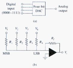
Digital-to-Analog Converter
The digital-to-analog converter (DAC) transforms digital signal into analog form. A typical example of a four-bit DAC is illustrated in [link](a). The four-bit DAC can be realized in many ways. A simple realization is the binary weighted ladder, shown in [link](b). The bits are weights according to the magnitude of their place value, by descending value of so that each lesser bit has half the weight of the next higher. This is obviously an inverting summing amplifier. The output is related to the inputs as shown in [link]. Thus,
Input is called the most significant bit (MSB), while input is the least significant bit (LSB). Each of the four binary inputs , …, can assume only two voltage levels, 0 or 1 V. By using the proper input and feedback resistor values, the DAC provides a single output that is proportional to the inputs.
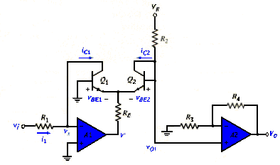
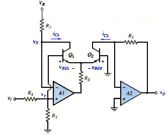
Instrumentation Amplifiers
One of the most useful and versatile op amp circuits for precision measurement and process control is the instrumentation amplifier (IA), so called because of its widespread use in measurement systems. Typical applications of IA include isolation amplifiers, thermocouple amplifiers, and data acquisition systems.
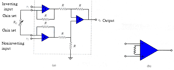
The instrumentation amplifier is an extension of the difference amplifier in that it amplifies the difference between its input signals. An instrumentation amplifier is shown in [link]. An instrumentation amplifier typically consists of three op amps and seven resistors.
We recognize that the amplifier in [link]. is a difference amplifier. Thus, from [link]. ,
Since the op amps and draw no current, current i flows through the three resistors as though they were in series. Hence,
But
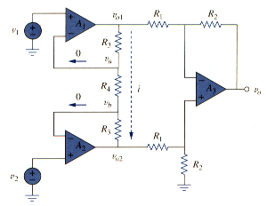
And , . Therefore,
Inserting [link]. and [link] into [link] gives
For convenience, the amplifier is shown again in [link](a), where the resistors are made equal except for the external gain-setting resistor , connected between the gain set terminals. [link](b) shows its schematic symbol. From [link] we have
Where the voltage gain is
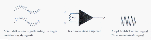
As shown in [link], the instrumentation amplifier amplifies small differential signal voltages superimposed on larger common-mode voltages. Since the common-mode voltages are equal, they cancel each other.
The IA has three major characteristics:
- The voltage gain is adjusted by one external resistor .
- The input impedance of both inputs is very high and does not vary as the gain is adjusted.
- The output depends on the difference between the inputs and , not on the voltage common to them (common mode voltage).
Due to the widespread use of IAs, manufacturers have developed these amplifiers on single package units. A typical example is the LH0036, developed by National Semiconductor. The gain can be varied from 1 to 1,000 by an external resistor whose value may vary from 100 to 10 k .
Log Amplifier
In this chapter, we have used linear passive elements in conjunction with the op-amp. If a nonlinear device, such as a diode, is used with an op-amp, a nonlinear transfer function is produced.
Consider the circuit in [link]. The diode is to be forward biased, so the input signal voltage is limited to positive values. The diode current is
If the diode is sufficiently forward biased, the (-1) term is negligible, and
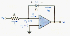
The input current can be written
And the output voltage is given by
Noting that , we can write
If we take the natural log of both sides of this equation, we obtain
[link] indicates that, for this circuit, the output voltage is proportional to the log of the input voltage. One disadvantage of this circuit is that the reverse-saturation current is a strong function of temperature, and it varies substantially from one diode to another.
The reverse-saturation current in [link] is eliminated in the circuit shown in [link], which uses two bipolar transistors instead of a single diode. However, the circuit is considerably more complicated than the diode current in [link].
Before we begin the analysis, we must first consider the two transistors, and . In order for the circuit to operate properly, the transistors must be biased in the active region. The collector current must therefore be positive, which implies that and must be positive. In turn, a positive input voltage means that the voltage at the inverting terminal is slightly positive, which produces a negative output voltage at . A negative forward biases both B-E junctions, and both and are biased in the active region.
With and biased “on”, assuming and are matched and at the same temperature, the collector currents are
And
where is reverse-saturation current in each transistor. If we take the natural log of both equations, we have
And
The B-E voltage of each transistor is then
And
For the noninverting terminal of op-amp , the input voltage with respect to ground is found by writing a KVL equation through the B-E junctions of and , as follows:
Substituting [link] and [link] into [link], we obtain
Or
Collector current is equal to ; therefore,
Neglecting the transistor base currents, collector current is
where is a reference voltage. Usually, we assume that
therefore,
Input voltage to op-amp is now
Since op-amp is a non-inverting amplifier, we have
Which becomes
For this circuit, the output voltage is directly proportional to the log of the input voltage. Note that the reverse-saturation currents for the two transistors cancel each other, which was one objective of this circuit. Experimentally, the circuit in [link] performs the log function over approximately four orders of magnitude of the input voltage, generally in the range of 2 mV < vi < 20 V.
To summarize the operation of the circuit in [link], we see from [link] that the collector current is essentially constant. A constant collector current implies a constant B-E voltage, that is, . On the other hand, input current is directly proportional to input voltage and, since , collector current is directly proportional to its corresponding input voltage. In this circuit, we apply a collector current and determine the resulting B-E voltage . Since is a constant, input voltage to op-amp is a direct function of , which in turn is proportional to the log of the input voltage.
Anti-log Amplifier
The complement, or inverse function, of the log amplifier is the anti-log or exponential amplifier, shown in [link]. The analysis for this circuit is similar to that of the log amplifier.
At the non-inverting terminal of , we have
[link] is that of a simple voltage divider, neglecting the base current into . The voltage at the non-inverting terminal of can also be written
Comparing [link] to [link] and [link], we see that
Collector current is
where
and we assume
Collector current can be written in terms of the output voltage, as follows:
Substituting the expressions for and into [link] and equating the two expressions for from [link] and [link], we can write
Solving for the log function, we have
Taking the exponential of both sides, we obtain
Finally, we have the output voltage, as follows:
For this circuit, the output voltage is an exponential function of the input voltage.
SUMMARY
- The op amp is a high-gain amplifier that has high input resistance and low output resistance.
Summary of basic op amp circuits.
- Table 3 summaries the op amp circuits considered in this chapter. The expression for the gain of each amplifier circuit holds whether the inputs are dc, ac, or time-varying in general.
- An ideal op amp has an infinite input resistance, a zero output resistance, and an infinite gain.
- For an ideal op amp, the current into each of its two input terminals is zero, and the voltage across its input terminals is negligibly small.
- In an inverting amplifier, the output voltage is a negative multiple of the input.
- In a non-inverting amplifier, the output is a positive multiple of the input.
- In a voltage follower, the output follows the input.
- In a summing amplifier, the output is the weighted sum of the inputs.
- In a difference amplifier, the output is proportional to the difference of the two inputs.
- Op amp circuits may be cascaded without changing their input-output relationships.
- Typical applications of the op amp considered in this chapter include the digital-to-analog converter, the instrumentation amplifier, log amplifier and anti-log amplifier.